Introduction Since Si3N4 possesses a hexagonal anisotropic structure with covalent bonding [1], its thermal conductivity exhibits strong anisotropy along the crystal axis. Pottier et al. succeeded in measuring the thermal conductivity of a single grain of β-Si3N4 by thermoreflectance microscopy [2]. The results showed that the thermal conductivity along the c-axis was 180 Wm-1K-1 and that along the a-axis was 69 Wm-1K-1. The anisotoropic thermal conductivity of Si3N4 crystal was demonstrated by using a molecular dynamics calculation by Hirosaki et al [3]. Each calculated ideal value along the c-axis of the hexagonal structure of Si3N4 was larger than that along the a-axis; each value includes thermal conductivity [4], elastic constant, phonon velocity, and phonon mean free path. In the previous work, the grain orientation of β-Si3N4 ceramic was controlled by a tape-casting and sintered by a hot-press and subsequently by HIP treatment. Anisotoropic thermal conductivity was observed in the bulk ceramic of β-Si3N4 with controlled grain orientation [4]. In this experiment, we tried to determine the orientation of each grain in Si3N4 ceramic with controlled grain orientation by two methods. A whole sintered body was analyzed by electron back-scattered diffraction (EBSD) with a scanning electron microscope. Detailed analysis was carried out by an electron diffraction method with a conventional transmission electron microscope (TEM). The degrees of tilting angle of each grain from the basis zone axis was calculated from the selected area diffraction (SAD) patterns, and these were expressed by tone of color and color variation, respectively. Furthermore, the microchemistry of the grain boundary was analyzed by energy dispersive spectroscopy (EDS). Here, we discuss the relationship between thermal conductivity and microstructure as well as the reason for the appearance of high thermal conductivity in the oriented Si3N4 ceramics. Experimental Procedure While the experimental procedure for the fabrication of a Si3N4 ceramic oriented by each grain has been described in detail elsewhere [4], it is mentioned only briefly here. α-Si3N4 powder with 5 mass% Y2O3 additive and 5 vol% rod-like β-Si3N4 as seed particles were mixed. The Si3N4 green sheet was produced by tape-casting, cutting and laminating at 100 MPa. The laminated specimens were hot-pressed at 2073 K for 2 h under 40 MPa unidirectional pressure in N2 flow. Then, the products were HIPed at 2773 K for 2 h under N2 gas pressure of 200 MPa. The EBSD method was carried by using a FE-SEM (JSM-7000 F, JEOL, Japan) equipped with an EBSD detector (TSL Inc.). The specimen was installed at a 70 degrees angle in the sample chamber. Crystallographic orientation of the grains was determined by scanning EBSD patterns [5]. A TEM foil was prepared using the standard technique for preparing the thin foils of ceramics: cutting, grinding, dimpling, Ar-ion thinning, and carbon coating to minimize the electric charging under the electron beam. Microstructural characterization of the product was performed with a TEM (JEOL-3000F) device, which makes it possible to provide electron probes with a full width at half maximum (FWHM) of around 0.5 nm and also with sufficiently high current for a point analysis by energy dispersive X-ray spectroscopy (EDS). Results The present sample is β-Si3N4 ceramics with highly oriented grains, as shown in Figure 1. Figures 1 (a) and (b) show SEM images taken from the directions parallel and perpendicular to the tape-casting direction, respectively. The grains grew up and were elongated by HIP treatment under 2773 K after fabrication by the tape-casting. TEM data showed that the c-axis of the large grain was parallel to the tape-casting direction, as shown in Figure 1(c). On the other hand, in Figure 1(b), idiomorphic grains were observed with an average diameter of about 8 μm, and the grains were affected by the hexagonal structure of β-Si3N4. The white contrast indicates that the amorphous phase precipitated from the liquid phase in the SiO2-Si3N4-Y2O3 system. We tried to determine the crystallographic orientation of the grains. First, EBSD method [5] was used to know the macrostructure of the ceramics. The EBSD method is rapid and allows greater sampling by using a SEM. Figure 1(d) shows an orientation-mapping image corresponding to that in Figure 1(b). Almost all of the grains were colored red in the EBSD image, which means the grain orientation was controlled in the [0001] direction by the tape-casting, except for the part of the grains of another color: e. g. purple or light blue. In some part of the area, however, a low-accuracy image was observed. It is not clear the grain boundaries due to the existence of the liquid phase between the grains, in which green or light yellow grains corresponded to the white contrast as an amorphous phase in Figure 1(b). 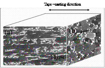
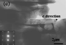 
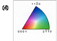
Figure 1. Photographs of β-Si3N4 fabricated by tape-casting, hot pressing and subsequent HIP sintering. (a) and (b) SEM images, (c) TEM image and SAD pattern, and (d) orientation-mapping by EBSD method. (Various colors are assigned to crystallographic orientations) Next, we determined more accurately the degrees of orientation for selected ten grains by conventional TEM. On the basis of the [0001] zone axis, the tilting angle was measured from the SAD pattern of each grain. Table 1 shows the orientation of each grain in β-Si3N4. The tilting angles of ϕ and θ are calculated by the following equations, respectively. ϕ = cos-1 (cos x⋅ cos y) …………..(1) θ = tan-1 ( ) ………………...(2) ) ………………...(2) x and y are measured angle along x-axis and y-axis, respectively in TEM device. φ is degree of tilting angle from the basis [0001] axis. θ is direction of tilting on the two-dimensional plane. Table 1. Orientation of each grain in β-Si3N4 ceramic determined by TEM. | | | 1 | -0.1 | -0.71 | 0.71 | 5.7 | -98.1 | 174.6 | | 2 | 7.1 | 1.5 | 7.26 | 58.0 | 12.0 | 8.0 | | 3 | -2.4 | 0.9 | 2.56 | 20.5 | 159.4 | 106.3 | | 4 | 7.1 | 1.8 | 7.32 | 58.6 | 14.3 | 9.5 | | 5 | -9.7 | 3.1 | 10.18 | 81.4 | 162.2 | 108.1 | | 6 | -19.3 | -5.2 | 19.96 | 159.7 | -164.6 | 130.3 | | 7 | -8.1 | 0.3 | 8.11 | 64.8 | 177.9 | 118.6 | | 8 | -13.6 | -3.7 | 14.09 | 112.7 | -164.6 | 130.3 | | 9 | -10.3 | -0.5 | 10.31 | 82.5 | -177.2 | 121.9 | | 10 | -8.4 | 7.0 | 10.92 | 87.3 | 140.0 | 93.3 | * Grain numbers correspond to the numbers in Figure 2. These degrees of φ and θ could be expressed by the tone of color and color variation, respectively. Figure 2 shows a TEM image and a colored image. Dark contrasts between the grains show the amorphous phase. Each grain oriented in various directions as indicated by the various colors, and the maximum tilting angle was 20 degrees in this area of the observed specimen, as indicated by the numbers in the colored image. The findings revealed that the orientation of each grain of β-Si3N4 was highly controlled by this synthesis procedure. 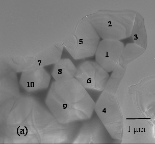
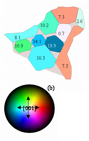
Figure 2. TEM image and orientation of each grain determined by electron diffraction method. The degrees of tilting angle of the grains are assigned to the tone of color, and the directions of tilting are assigned to color variation. Figure 3 shows a TEM image at a two-grain junction (No. 2 and No. 5 in Figure 2) and chemical composition data obtained from the grain boundary region. Inset is a SAD pattern taken from two grains. Those two grains were slightly tilted from the [0001] zone axis with an amorphous boundary film between them. The thickness of the intergranular film was <1 nm, which was formed by liquid-phase sintering with Y2O3 additive [6, 7]. 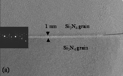
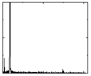
Figure 3. (a)TEM image and (b) EDS spectra of grain boundary between grain 2 and grain 5. Inset is SAD pattern obtained from two grains at boundary. Discussion Table 2 shows thermal conductivity values of Si3N4 obtained by various methods. (The value of No.4 corresponds to the present material.) Table 2: A comparison of the thermal conductivity values for Si3N4 ceramics. | | | 1 | MD simulation at 300 K3) | 170 | 450 | 2.65 | | 2 | Single crystal grain (experimental results)2) | 69 | 180 | 2.61 | | 3 | Tape-casting and hot press (experimental results)4) | 30 | 70 | 2.33 | | 4 | Tape-casting, hot press and HIP (experimental results)4) | 52 | 155 | 2.98 | | 5 | MD simulation at 300 K for  -Si3N4 3) -Si3N4 3) | 105 | 225 | 2.14 | Thermal conductivity is closely related to the crystal structure. The difference of the thermal conductivity between α- and β-Si3N4 is caused by stacking sequence along the c-direction, in which Si-N layers are stacked as ABCD….ABCD in α-Si3N4 and AB…AB in β-Si3N4 [7]. The difference between the simulated and experimental values was caused by the following factors; defects of grain, amorphous phase at the grain junction, impurities, etc [8]. The ratio of the thermal conductivity values for β-Si3N4 along the c- axis versus a-axis (c/a) was in a range of 2.33 to 2.98, as shown in Table 2. The result revealed that anisotoropic thermal conductivity of each grain greatly impacted the bulk-ceramic fabricated by the tape-casting. We noticed the differences in values between No. 3 and No. 4, which was before and after HIP process. In the previous paper [4], differences in grain size were observed between before and after HIP treatment. However, the thermal conductivity at room temperature is independent of grain size as previously reported by Watari et al [9]. The reason for this could be that the phonon mean free path is shorter than the grain size. The grain size is of the order of 1 μm, while the ideal phonon mean free path of β-Si3N4 is calculated to be 23 nm and 52 nm along the a- and c- directions, respectively [2]. Therefore, the difference between No. 3 and No. 4 was caused from the difference in degree of purity for the grains. In other words, internal defects of grains were decreased during the HIP treatment. Mitomo reported [7] each step of liquid-sintering process for Si3N4, in which small β-Si3N4 powders melt and precipitate on the large β-Si3N4 grain by a gas pressure sintering above 2023 K. We considered that impurities dissolved in the liquid phase and pure Si3N4 was precipitated, and the large grain became larger. Favored axis of grain growth in the Si3N4 grain is c-axis of the hexagonal structure [5]. As a result of controlling the orientation of each grain, the grain sizes became extremely long along the c-direction. In the case of the Si3N4, the thermal conductivity is lower than that of SiC with BeO additive [10] and AlN with Y2O3 additive [11]. The reason for this is existence of large amount of amorphous material at the multi-grain junction, which has a short phonon mean free path, resulting in a low thermal conductivity. However, the liquid phase at the grain boundary contributed to the grain orientation effectively [12]. Therefore, the anisotropy in thermal conductivity for each grain affected greatly that of bulk-material oriented grains. Conclusion Anisotropy in thermal conductivity was exhibited in β-Si3N4 when each grain was oriented by tape-casting, followed by hot-pressing and HIPing at 2773 K. The crystallographic orientation of each grain could be determined by EBSD method and electron diffraction method. As a result, each grain was highly oriented within 20 degrees from the basic [0001] axis in the TEM observed specimen. It was assumed that this was achieved effectively by liquid-phase sintering. The results showed that the anisotropy in thermal conductivity for each grain affected greatly that of the bulk-material oriented grains by tape-casting. Furthermore, the grain grew along the favored direction, the c-axis, during the dissolution-precipitation mechanism in the liquid-phase sintering by HIP treatment at 2773 K. During the grain growth, impurities in the grains decreased, and, as a result, high-thermal conductivity appeared in the β-Si3N4 ceramics with highly oriented grains. References 1. M. Mamoru, “Liquid phase sintering of silicon nitride”, M. Ceramics, 30 (5) (1995) 395-398 [in Japanese]. 2. B-C. Li, L. Pottier, J. P. Roger, D. Fournier, K. Watari and K. Hirao, “Measuring the Anisotropic Thermal Diffusivity of Silicon Nitride Grains by Thermoreflectance Microscopy,”, J. Euro. Ceram Soc., 19 (1999) 1631-39. 3. N. Hirosaki, S. Ogata, C. Kocer, H. Kitagawa and Y. Nakamura, “Molecular dynamics calculation of the ideal thermal conductivity of single-crystal α-and β-Si3N4”, Physical Review B, (65) (2002) 134110. 4. K. Watari, K. Hirao, M. Brito, M. Toriyama and S. Kanzaki, “Hot isostatic pressing to increase thermal conductivity of Si3N4 ceramics”, J. mater. Res., 14 (4) (1999) 1538-1541. 5. Y. Yasutomi, Y. Sakaida, N. Hirosaki and Y. Ikuhara, “Analysis of Crystallographic Orientation of Elongated β-Si3N4 Particles in in situ Si3N4 Composite by the Electron Backscattering Diffraction Method,” J. Ceram. Soc. Jpn., 106 (1998) 980-83. 6. H. –J. Kleebe, “Structure and chemistry of interfaces in Si3N4 Ceramics studied by transmission electron microscopy”, J. Ceram. Soc. Jpn., 105 (6) (1997) 453-475. 7. M. Mitomo, “Progress in silicon nitride and sialon ceramics”, Ceramics, 38 (9) (2003) 668-685 [in Japanese]. 8. K. Watari and H. Nakano ” Microstructure and thermal conductivity mechanism of high thermal conductivity AlN ceramics”, Ceramis, 39 (9) (2004) 678-683 [in Japanese]. 9. 9. K. Watari, K. Hirao, M. Toriyam and K. Ishizaki, “Effect of grain size on the thermal conductivity of Si3N4”, J. Am. Ceram. Soc., 82 (3) (1999)777-79. 10. 10. H. Nakano, K. Watari, Y. Kinemuchi, K. Ishizaki and K. Urabe, “Microstructural characterization of high-thermal –conductivty SiC ceramics”, J. Europ. Ceram. Soc., 24, (2004) 3658-3690. 11. 11. H. Nakano, K. Watari, Y. Kinemuchi, H. Hayashi and K. Urabe, “Microstructural characterization of high-thermal–conductivity aluminum nitride ceramic”, J. Am. Ceram. Soc., 85 (12) (2002) 3093-95. 12. 12. S. Igarashi, “Denshi ceramics no ryushi haikou gizyutu”, Electronic ceramics, 7, (1991) 4-10 [in Japanese]. Contact Details | Hiromi Nakano
Electron Microscope Laboratory Ryukoku University
Seta, Otsu
520-2194
Japan E-mail: [email protected] | Hiroshi Nakano
Department of Applied Mathematics and Informatics Ryukoku University
Seta, Otsu
520-2194
Japan | | Koji Watari National Institute of Advanced Industrial Science and Technology
Ceramic Research Institute
Moriyama-ku
Nagoya 463-8560
Japan | | |