Sponsored by HORIBAOct 18 2013
A LabRAM HR 800 (HORIBA) spectrometer in conjunction with an inverted microscope (Olympus IX 71) and a X,Y Piezoelectric stage was used to record Raman measurements. The X,Y Piezoelectric stage positions samples with good accuracy and precision.
Experimental Procedure
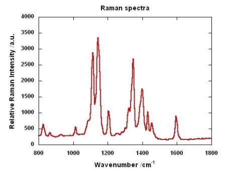
Figure 1. Raman Spectra of azobenzene polymer with an acquisition time of 5s
A 100X, 0.9 NA microscope objective was utilized in this experiment. As shown in Figure 1, A Raman spectrum was captured every 100nm along the X and Y directions at 5s integration time per spectrum (λ excitation=752.4nm). Raman image from a periodically structured azobenzene-containing polymer thin film (300nm) with a periodicity of ~1µm is illustrated in Figure 2.
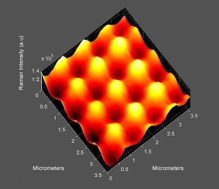
Figure 2. Raman image from a periodically structured azobenzene-containing polymer thin film
The difference of the Raman intensity over the X and Y directions is depicted in Figure 3, showing the integration of the Raman signal over the spectral domain of 1060-1180cm-1. It must be noted that the information on the Raman profile is acquired with a spatial resolution superior than λ/2 (at the diffraction limit).
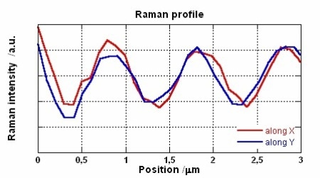
Figure 3. Variation of the Raman intensity over the X and Y directions
Inscription of the two-dimensional grating
The surface has been structured with holographic techniques in a one step procedure along the X and Y directions. Neither wet nor photocuring processing is used. A grating is first inscribed with grooves along the X direction and the sample is subsequently rotated by 90°. Now the second grating is inscribed with grooves along the Y direction. The intensity of the first diffracted orders is analyzed to have the same intensities in both X and Y directions.
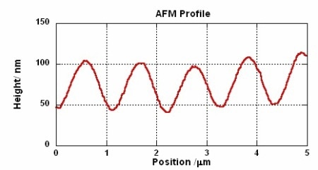
Figure 4. AFM Profile of the Height Variations
AFM images illustrated in Figure 4 show a periodic structure on large surfaces with an amplitude range of 50-110nm. AFM images in 3D and 2D representations are shown in Figure 5.
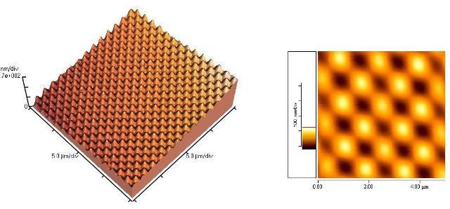
Figure 5. AFM images in 3D and 2D representations

This information has been sourced, reviewed and adapted from materials provided by HORIBA.
For more information on this source, please visit HORIBA.