The Digital Pulsed Force Mode (DPFM) provides new insights into nanoscale materials research. It can store the full tip-sample interaction in the event of an AFM imaging process, thereby enabling users to record energetic and mechanical properties in conjunction with the topography.
However, extracting real physical properties from AFM measurements is often a challenging task because of the changes in the conditions during a measurement and continuous changes in the shape of the cantilever tip, etc. The inclusion of a reference in the imaging area for material characterization can compensate for all these uncontrollable parameters.
Nanoscale Characterization of Rubber Compounds with DPFM
This article presents the results of nanoscale characterization of two rubber compounds, which were analyzed as thin films of polymer blends in conjunction with PMMA. The thin films were formed by the spin-coating of polymer solutions on glass substrates. Figure 1 illustrates the topography of thin films of SBR-PMMA and SBS-PMMA on glass substrates.
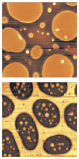
Figure 1. Topography of polymer blends: Top: SBR-PMMA (image size 7x7x0.03µm3) Bottom: SBS-PMMA (image size 10x10x0.08µm3).
Confocal Raman Microscopy measurements have revealed that the higher topographical features represent PMMA. Typical Pulsed Force curves acquired from PMMA and SBR in the SBR-PMMA blend are depicted in the top picture and from PMMA and SBS in the SBS-PMMA blend in the bottom picture of Figure 2, respectively.
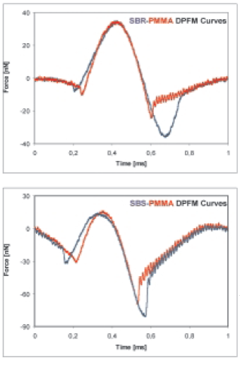
Figure 2. Typical Pulsed Force Curves obtained from the two polymer films.
The adhesion maps recorded stored along with the topography images illustrated in Figure 1 are shown in Figure 3.
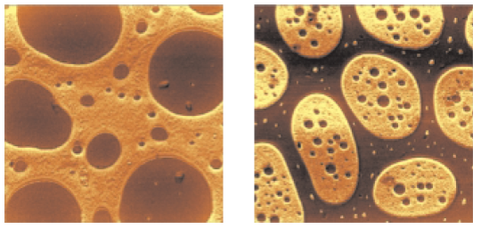
Figure 3. Adhesion maps of the thin film of SBR-PMMA (left) and SBS-PMMA (right).
The difference in adhesion forces of the two polymer blends was estimated as shown below:
Δ A1 = ASBR - APMMA = kS(Vad(SBR) - Vad (PMMA) ) = 10 ± 3 nN (1)
Δ A2 = ASBS - APMMA = kS(Vad(SBS) - Vad (PMMA) ) = 11 ± 3 nN (2)
Where, cantilever spring constant k = 2.8N/m; Sensitivity S = 200nm/V; and Vad(SBS), Vad(SBS), and Vad(PMMA) are the measured voltages on the adhesion outputs of the DPFM electronics. This data is insufficient to corroborate the blending of the two different polymers with PMMA. The stiffness maps for the two thin films are depicted in Figure 4.
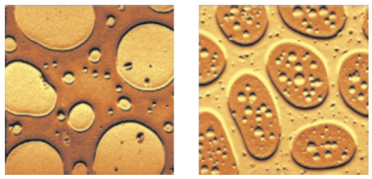
Figure 4. Stiffness maps of the thin film of SBR-PMMA (left) and SBS-PMMA (right).
The difference in stiffness of the two polymer blends was computed as follows:
Δ S1 = SPMMA - SSBR = kS(Vstiff(PMMA) - Vstiff (SBR) ) / Δ z = 2.5 ± 0.3 N/m (3)
Δ S2 = SPMMA - SSBS = kS(Vstiff(PMMA) - Vstiff (SBS) ) / Δ z = 0.6 ± 0.3 N/m (4)
Where, Δz represents the tip penetration depth; and Vstiff(PMMA) , Vstiff(SBR) , and Vstiff(SBS) are the measured voltages on the stiffness output of the DPFM electronics. Since both thin films consist of the reference PMMA, the stiffness difference estimated in Equations 3 and 4 is correlated to various stiffness properties of the SBR and SBS. The stiffness ratio (Δ S1/Δ S2) of 4 demonstrates that the SBR is softer than SBS by a factor of 4.

This information has been sourced, reviewed and adapted from materials provided by WITec GmbH.
For more information on this source, please visit WITec GmbH.