Photovoltaic Materials - Silicon

Background

Silicon is still the most popular solar-cell material for commercial applications because it is so readily abundant (it is actually the second most abundant element in the Earth's crust-second only to oxygen!). However, to be useful in solar cells, it must be refined to 99.9999% purity.

In single-crystal silicon, the molecular structure of the material is uniform because the entire structure is grown from the same or a "single" crystal. This uniformity is ideal for efficiently transferring electrons through the material. To make an effective PV cell, silicon is "doped" to make it n-type and p-type. Semicrystalline silicon, on the other hand, consists of several smaller crystals or "grains," which introduce "boundaries." These boundaries impede the flow of electrons and encourage them to recombine with holes and thereby reduce the power output of the cell. However, semicrystalline silicon is much cheaper to produce than single-crystalline silicon, so researchers are working on other ways of minimizing the effects of grain boundaries.

Different Structures

Figure 1. Single-crystal material (a) is structurally uniform; there are no disturbances in the orderly arrangement of atoms. Semicrystalline material (b) is made up of several crystals or "grains." At the interfaces of the grains, or "boundaries," the atomic order is disrupted. Here, electrons are more likely to recombine with holes rather than contribute to the electrical circuit.

Even very small crystals of silicon can make successful solar cells, and R&D is being performed on polycrystalline silicon in hopes of making the material suitable for cost-effective solar cells. Polycrystalline material contains many single crystals about the thickness of a human hair, or about 1/1000 the size of the crystals in semicrystalline material.

Preparing Single-Crystalline Material

To change it into the single-crystal state, we first melt the high-purity silicon. We then cause it to reform very slowly in contact with a single crystal "seed." The silicon adapts to the pattern of the single crystal seed as it cools and solidifies gradually. Not surprisingly, because we start from a "seed," this process is called "growing" a new ingot of single-crystal silicon out of the molten silicon. Several specific processes can be used to accomplish this. The most established and dependable means are the Czochralski method and the floating-zone (FZ) technique.

In the Czochralski process, a seed crystal is dipped into a crucible of molten silicon and withdrawn slowly, pulling a cylindrical single crystal as the silicon crystallizes on the seed.

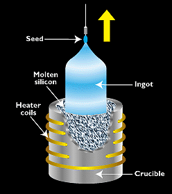
Figure 2. - The most widely used technique for making single-crystal silicon is the Czochralski process, in which seed of single-crystal silicon contacts the top of molten silicon. As the seed is slowly raised, atoms of the molten silicon solidify in the pattern of the seed and extend the single-crystal structure

The Float Zone Process

The float zone (FZ) process produces purer crystals, because they are not contaminated by the crucible as Czochralski crystals are. In the FZ process, a silicon rod is set atop a seed crystal and lowered through an electromagnetic coil. The coil's magnetic field induces an electric field in the rod, heating and melting the interface between the rod and the seed. Single-crystal silicon forms at the interface, growing upward as the coils are slowly raised.

Once the single-crystal ingots are produced, the must be sliced to form wafers.

Although single-crystal silicon technology is well developed, the Czochralski, FZ, and ingot-casting processes are complex and expensive. A group of new crystal-producing processes, however, generally called shaped-ribbon growth, could reduce processing costs by forming silicon directly into thin, usable wafers of single-crystal silicon. These methods involve forming thin crystalline sheets directly, thereby avoiding the slicing step required of cylindrical ingots.

Semicrystalline Material

Semicrystalline silicon can be produced in a variety of ways. The most popular commercial methods involve a casting process in which molten silicon is directly cast into a mould and allowed to solidify into an ingot. Generally, the mould is square, producing an ingot that can be cut and sliced into square cells to fit more compactly into a PV module. (Round cells leave space between them, where square cells can fit together with a minimum of wasted space).

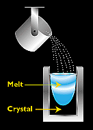
Figure 3. - The most popular method for making commercial semicrystalline silicon is casting, in which molten silicon is poured directly into a mould and allowed to solidify into an ingot.

Source: U.S. Department of Energy Photovoltaics Program.

For more information on this source please visit National Renewable Energy Laboratory

Tell Us What You Think

Do you have a review, update or anything you would like to add to this article?

Leave your feedback
Your comment type
Submit

While we only use edited and approved content for Azthena answers, it may on occasions provide incorrect responses. Please confirm any data provided with the related suppliers or authors. We do not provide medical advice, if you search for medical information you must always consult a medical professional before acting on any information provided.

Your questions, but not your email details will be shared with OpenAI and retained for 30 days in accordance with their privacy principles.

Please do not ask questions that use sensitive or confidential information.

Read the full Terms & Conditions.