This article deals with the accurate and quick measurements of depth, flatness and width, of closed channel microfluidic devices, follwing fabrication. The words “Practical Microfluidics” found on the cover of the March 2014 issue of Nature reveal that microfluidics technology is becoming a mainstream technology. According to ResearchAndMarkets.com, the global micro fluidics was estimated at US$3 billion in 2015. However, some manufacturing challenges remain for quality assurance, since the microfluidic device fabrication is often not connected with the end-users.
Quality in Micro Fluidic Devices — A Challenge for Traditional Microscopy
Microfluidics operate on the basis of specific pressure points, flow dynamics and mixing streams, all of which need correct volume and flow simulations. However, during device manufacture, precision is influenced by mating practices, surface treatments, surface roughness, and material spoilage caused during fabrication practices. It is almost impossible to match pre-production simulation with post-production performance. Finding out the reason for the mismatch requires determining precise measurements of the fabricated device.
Moreover, R&D devices are usually glass-based devices, but mainstream fabricated devices use soft materials such as PDMS. Hence, it is a big challenge to maintain similar geometries on PDMS. For optimizing the evolution from R&D to production, it is necessary to achieve the capability for measuring closed microfluidic devices on PDMS and glass. For microfluidic devices, conventional quality methods using profiler probes or optical microscopy to validate the specifications are not successful (Figure 1). These methods are not convenient to measure large dimensions in the XY directions as well as substrates measuring only in millimetres. In addition, fast and specific quality control processes need to be developed to determine if a product conforms to the required specifications.
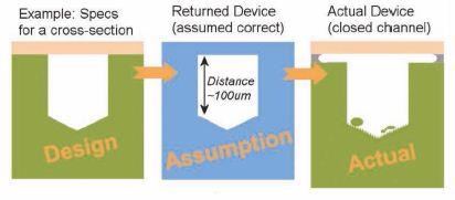
Figure 1. Microfluidic Device Challenges for Traditional Quality Microscopy Methods, as shown on a cartoon representation of a Micro fluidics Device cross-section.
Microfluidic devices are three-dimensional in nature, which also possess challenges for techniques relying on probes. Trenches may be up to hundreds of microns in-depth, so quality processes have to measure the distance as well as the depth of the trench. A method to examine a closed trench is also needed, as, after assembly, the finished device will also be subject to quality control.
Figure 2 shows the three particular challenges that arise for quality methodologies employing conventional microscopy.
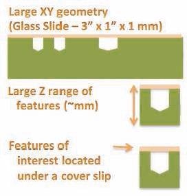
Figure 2. Microfluidic device challenges for traditional quality microscopy methods, as shown on a cartoon representation of a microfluidics device cross-section.
Microfluidic devices have large XY geometry as they are as big as a glass slide, which in terms of microscopy, is deemed as quite large. A requirement for quality process is analyzing specifications across a chip device, which, however, can be painstaking and time-consuming.
As microfluidics channels often move more than just fluid and cells, the Z-axis dimensions can be quite significant, if they are in the millimetre range. Since for quality processes, measurements at the end of the processes are vital, this can involve looking inside a microfluidic device.
Microscopy Solution Requirements for Quality Control
The specific criteria that should be satisfied by quality processes for microfluidic devices are:
- Be non-contact and non-destructive – The demands of the medical industry are such that once the device is manufactured, contact with any other surface should be minimal. Hence, contact profilometers would be unable to analyze the interiors of a closed channel.
- Cost Effective – In contrast to the semiconductor industry, the expenditure incurred for a microfluidic device does not mean that a large amount of money can be invested in metrology equipment. Any quality process tool utilized for the measurements has to be economically viable too.
- Optical – Two out of the three materials (polymers and glass) that are typically used for microfluidics are transparent to white light, indicating that an optical technique is a cost-effective measurement technology. The optical technique can also be used for silicon-based devices.
- Fast – In a production environment, rapid quality checks are necessary. Only a few minutes should be spent to evaluate whether a device meets or exceeds the specifications.
Quality Control of Finished Micro Fluidic Devices
In 2009, James Xu and Ken Lee, metrology industry veterans, developed the Confocal Grid Structured Illumination (CGSI) technique. The CGSI technique evolved confocal microscopy to allow measuring difficult surfaces and imaging in true color. In addition to being used for various surface analysis applications, the CGSI technique can be inimitably used for imaging sealed microfluidic devices (Figure 3).
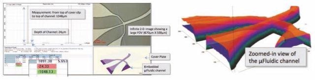
Figure 3. Measurement of the depth of a channel (above) on a closed ‘lab-on-a- chip’ device. This optical technique allows a large XY area (over a half-mm2) & deep Z height (over 1 mm deep to the channel) in a single scan as well as providing multi-surface imaging (right). Images courtesy of KLA.
Many improvements in the CGSI technique, referred to as ZDots on the Zeta-20 Optical Profiler, enable the “see-into-a-closed-channel” ability (Figure 4). Two case studies and two application examples are presented in this article for demonstrating this feature.
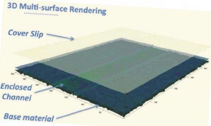
Figure 4. High light throughput optical design images multiple layers simultaneously in less than a minute. Image Courtesy of KLA.
Case Studies
Animal Reproduction
Organisation: A company utilizing microfluidics in animal reproduction
Situation: The chip was designed by the company, and was sent out for fabrication. The fabricator returned the chip, apparently made according to the specifications. The supplier company as well as the end-use customer did not have a tool for measuring the actual dimensions of the device after fabrication.
Problem: For unknown reasons, the device did not perform according to the simulation.
Solution: By utilizing the CGSI (ZDot) technique on a Zeta-20 Optical Profiler, the company determined the reason in less than 15min by performing multiple scanning. The reason was that the component was not fabricated as per the specifications. Additionally, the fabricator had used mechanical polishing process, which resulted in significant device-to-device variation.
Collapsed Channels
Organisation: A university fabrication team
Situation: The team fabricates devices for several internal and external customers. The devices are developed in many forms ranging from prototypes to those fabricated for pilot developments. The finished devices failed to perform according to customers’ specifications.
Problem: The team could not identify the problem as it was not able to measure closed microfluidic devices.
Solution: Analysis of closed cells by using the CGSI technology showed the collapse of PDMS in some locations, as shown Figure 5.
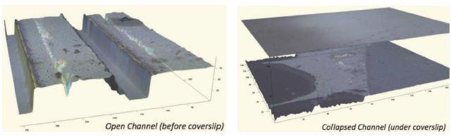
Figure 5. Images showing a channel before and after application of cover slip, in a microfluidic device made via photolithography in PDMS, then covered with a flat piece of PDMS. After the application of the coverslip, the channel collapsed. While easily visible on this Zeta-20 Optical Profiler using CGSI technology, the collapsed channel had previously been a mystery to the university lab fabricators. Images Courtesy of KLA.
Application Examples
Deep Trench
Application: Measuring an Open Trench (no coverslip)
Need: To measure the precision of the etching step for quality purposes, and as an accept/reject quality check gate for subsequent processing
Planned depth: 300µm
Actual depth: 296.5µm (Figure 6)
The accuracy of the CGSI technique is up to ±10nm. Quality process for this application is generally not possible by using other profiling technologies.
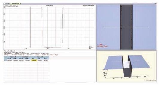
Figure 6. Application example of the measurement of a deep trench. Image courtesy of KLA.
Accuracy of the CGSI (ZDot) Method
The measurement made by a CGSI measurement technique is compared against that made by a stylus profilometer using a solder bump on a passivated, transparent substrate. The stylus profilometer measures 76.91µm, whereas the CGSI instrument (Zeta-20 Optical Profiler) measures 77.33µm. Figure 7 shows the results of the contact profiler and the optical profiler. Correlation is better than 50nm. Measurements of this type i.e. measurement over a centerpoint of a half-sphere, usually require several passes of a stylus profilometer so as to verify that the highest point has been actually reached, thus resulting in increased time-consumption. For optical profilers, which do not use ZDots, the arrangement of a shiny solder bump on a passivated, transparent substrate can present considerable imaging challenges.
By utilising an instrument that employs the CGSI technique, quick and accurate measurements are ensured. The CGSI (ZDot) technology ensures quality control of microfluidic device manufacturing process, such as verifying of those measurements after the closure of the device channels.
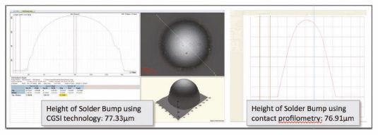
Figure 7. Comparison of the accuracy of the CGSI imaging method with contact profilometry, using both to image a solder bump on a passivated, transparent substrate. Images courtesy of KLA.

This information has been sourced, reviewed and adapted from materials provided by KLA Corporation.
For more information on this source, please visit KLA Corporation.