|
GaN-based LEDs and power electronics are currently a very active area for research, development, and production. While accurate and reproducible substrate temperature measurement is imperative for improved process control, and ultimately better device performance, current technology is insufficient for accurate and reproducible wafer temperature measurement. All forms of pyrometry, including emissivity-corrected pyrometers (ECPs), rely upon technology that measures black body radiation from the sample, which occurs at wavelengths that are transparent to GaN and SiC materials due to their large band gap. Therefore, all current temperature measurements are based upon the radiation from the heater or the susceptor (in MOCVD) behind the sample, and do not make a direct temperature measurement of the sample itself.
One of the key strengths of the kSA BandiT system is that it measures a fundamental material property of the wafer, namely the temperature-dependent band gap. This measurement is manifested through the monitoring of the absorption edge of the material and is NOT intensity dependent, as is a pyrometer reading. In the case of GaN deposited on sapphire, kSA BandiT measures the temperature of the GaN film itself and not that of the susceptor, heater, or substrate. (Sapphire is an insulator and does not have a band gap.) Since SiC is a semiconductor with similar band gap to GaN, the same hardware may be used when using SiC as a substrate for GaN-based films. As such, the measurement is not affected by changing view port transmission, stray IR sources, changing reactor emissivity, and so on. In addition, never before measured changes in temperature due to gas flow convection or substrate bowing are now possible, yielding a novel method for measuring the true temperature of GaN epiwafers.
Band Edge Technology
The kSA BandiT is a non-contact, non-invasive, real-time, absolute wafer temperature sensor utilizing the temperature-dependent absorption edge of semiconductor materials to determine substrate temperature. The absorption edge position is directly related to the band gap energy of the material, which, in turn, is temperature dependent. While both empirical and theoretical equations exist for band gap dependence on temperature for most materials of interest, in practice these equations do not consider doping effects, scattering, and instrument response. As a result, it is much more accurate to generate experimental calibration curves or lookup tables that map a measured absorption edge wavelength to a previously calibrated temperature value. k-Space has developed an empirical method for calibrating the band edge temperature dependence of a particular wafer with that of a calibrated thermocouple directly mounted to the sample (Figure 1). Subsequent temperature measurements using the BandiT system are based upon this direct temperature vs. band edge relationship.
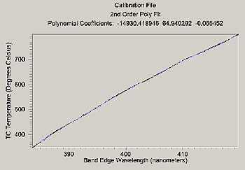
Figure 1. kSA BandiT Calibration for GaN.
Chamber Mounting Options
The kSA BandiT can be operated in two modes:
1. Reflection mode: (shown in Figure 2) A broadband light source is mounted along with the BandiT detector at nonspecular angles. This configuration is for monitoring traditional materials requiring band edge versus temperature detection at shorter wavelengths (i.e. GaN, SiC, ZnO) via a tailored spectrometer. Both dual port and single port options are available to suit most commercial MBE and MOCVD reactors.
2. Transmission mode: The substrate heater is used as the light source for band edge versus temperature applications covering the IR spectral range (i.e. GaAs, InP, & Si). A secondary light source is not required.
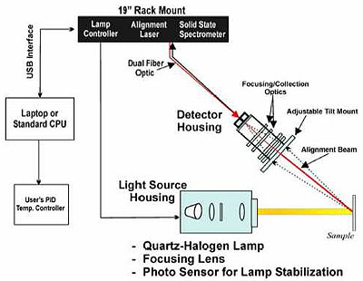
Figure 2. kSA BandiT Two-Port Reflection Mode Configuration.
Conditioning for GaN Use
The kSA BandiT response in the short wavelength regime is nonlinear, meaning the light source has lower output power and the spectrometer has lower sensitivity at the shortest wavelengths (380-520 nm). To resolve this issue, the instrument response must be divided out of the signal to see a clear absorption edge. This is done by taking a room temperature reference spectra with the lamp set to the power level that will be used during subsequent temperature monitoring. The spectra acquired from the sample is then divided by the reference spectra in order to obtain the absorption edge position. The absorption edge is clearly seen after the reference divide and subsequent processing (Figure 3). The system is now ready for GaN film temperature monitoring.
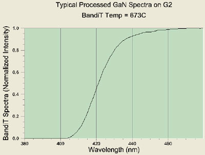
Figure 3. Processed MOCVD GaN Spectra.
GaN BandiT MOCVD Configuration
The GaN BandiT system was mounted on an Aixtron G2 MOCVD reactor, modified for GaN growth (Figure 4). The light source and detector were engineered to facilitate mounting onto a single 1.33” CF or similar view port at normal incidence to the wafer surface. The light source used was a modified liquid light guide apparatus which enabled excellent coupling of the broadband light to the growth surface. Due to the rough backside of single-side polished sapphire substrates (SSP) and close proximity to the wafer surface, there was a strong diffuse signal for analysis. The resulting band edge signal was not affected by the planetary rotation of wafers within the system.
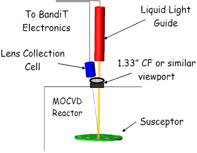
Figure 4. MOCVD GaN BandiT Configuration.
MOCVD Growth Results
In order to evaluate kSA BandiT for MOCVD growth, the system was tested under various conditions encountered during optical device growth (i.e. HBLEDs and laser diodes). This included a temperature ramp to growth temperature, GaN and InGaN deposition, and subsequent analysis of individual wafer temperature information.
The Aixtron G2 MOCVD reactor tested had 9 wafer positions on the susceptor and was typically rotated at 6-10 rpm. The G2 features gas foil rotation, so each wafer rotates rapidly with its holding pocket, in addition to the slower rotation speed of the entire susceptor. The kSA GaN BandiT was able to spatially resolve temperatures from all wafers during rotation. The data acquired shows that the gas foil rotation has no bearing on the absolute BandiT temperature measurement. This result is to be expected because the diffuse reflectance method is not sensitive to angular variation, especially on SSP substrates.
Figure 5 shows BandiT data during a temperature ramp. Note that the apparent noise in the data is not noise at all, but rather variations in temperature between wafers (see inset). The data taken here shows approximately 12 temperature measurements per wafer, yielding spatially resolved temperature measurement. Note that the temperature profiles shown in Figure 5 are repeatable over longer time scales than those shown here.
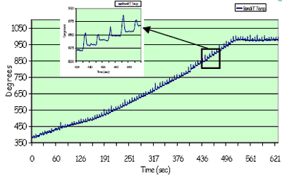
Figure 5. MOCVD temperature ramp and stabilization with multi wafer temperature detection.
In order to observe the effect more closely, individual wafer temperature data was extracted from the BandiT software to yield the spatially resolved temperature information. Data was taken during rotation for a constant thermocouple (TC) and pyrometry temperature of 950 degrees C. The BandiT system was configured to take 12 measurements per wafer at 6 rpm. While constant temperature was measured with both the TC and pyrometer, Figure 6 shows a clear thermal gradient from edge (10 degrees hotter) to center (cooler with localized hot spots). These results were most likely from the physical contact variations between the substrate and the susceptor. BandiT was able to process the data and throw away signal coming from the platen or from empty positions within the platen, resulting in temperature data from wafers only, which were not affected by mechanical ‘walking’ of the wafer or susceptor positions.
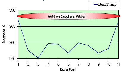
Figure 6. 3” Spatially resolved wafer surface temperature during MOCVD planetary rotation.
Since InGaN has a smaller band gap than GaN (expected to absorb the GaN signal), 1000 Å of material was grown to validate continued observance of a strong band edge signal required for temperature measurement. The data in Figure 7 shows no change in temperature during the deposition, which is to be expected due to the absence of additional IR absorption from the InGaN layer compared to the GaN layer. The data shown here is a subset of a longer data set that shows the same temperature profile. A total of 1000 Å of InGaN was deposited. Note that the raw BandiT spectra signal was decreased by about 20% during the deposition of the InGaN layer (due to absorption from the smaller band gap overlayer), but this did not affect the BandiT temperature determination as the calculation is not signal-level dependant. Interestingly, during the InGaN deposition, kSA BandiT actually measured a slight temperature increase at the wafer surface vs. a decrease read via the pyrometer, which is consistant with the expected outcome vs. the false reading from the pyrometer.
Figure 7. 1000 Å InGaN growth on single wafer GaN. Temperature gradients across wafer yield oscillations.
Finally, temperature data was extracted for two separate wafers to illustrate how BandiT would be used in a production MOCVD system (see Figure 8). Since BandiT is able to optically resolve multiwafer temperatures, individual wafer temperatures at any point on the wafer can be measured, sorted, and output to the appropriate control system.
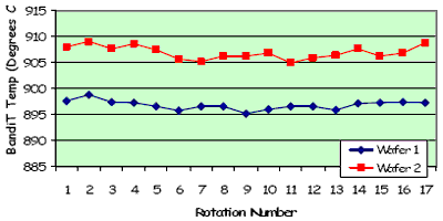
Figure 8. Wafer center point temperature extracted for two separate wafers on susceptor.
MBE Growth Results
The GaN BandiT system was tested on a Veeco GEN 200 MBE reactor equipped with an RF Nitrogen plasma source and solid source effusion cells. The standard light source was mounted on a 2.75” view port at normal incidence to the substrate, and the detector was mounted on a 2.75” view port at ~ 18° degrees with respect to the normal of the substrate, as shown in Figure 9. After conditioning the system for use with GaN, data was gathered for both GaN on sapphire and SiC substrates.
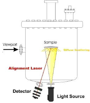
Figure 9. BandiT mounted on Veeco GEN200 MBE.
Typical data during 50C ramp intervals is shown in Figure 10. Note that although the TC reading is stable at each plateau, the actual sample temperature decreases during the soak time.
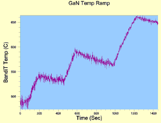
Figure 10. MBE GaN temperature measurement during 50ºC ramps.
BandiT data was acquired during GaN deposition to determine the effect of the Gallium source and RF Nitrogen plasma source on the temperature measurement. Figure 11 shows the pre-growth temperature ramp of the GaN template, then a cooling, and finally the commencement of deposition at 2395 seconds. There was no difference in the temperature data when the growth commenced. Note also that an initial ~ 5 seconds of pure Gallium growth occurs before the Nitrogen plasma is opened, to ensure wetting of the surface so subsequent stoichiometric GaN can be grown. This initial Gallium wetting also does not effect the BandiT measurement. Temperature was monitored for 2.3 hrs during deposition, corresponding to approximately 1.2µm of additional GaN film. We saw no appreciable change in temperature, indicating that there was no significant change in absorption due to additional GaN material.
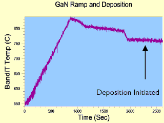
Figure 11. GaN deposition with no change in temperature signal.
For those using SiC wafers for GaN MBE, we also evaluated double-side polished 6H SiC substrates with a metal back coat. The DSP surface acted like a mirror, reflecting much of the incident light. However, by using the same methodology of reference dividing the background, a clear band edge was observed for direct temperature measurement via the SiC substrate itself (see Figure 12). Since the band gap of SiC is similar to that of GaN, the same BandiT system hardware may be used.
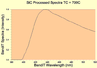
Figure 12. DSP 6H BandiT Absorption Spectra.
Summary
This study has shown a novel GaN wafer surface temperature measurement capability for MBE and MOCVD with the kSA BandiT system. Never before has a technique been able to measure temperature variations at the GaN surface level in real time. This approach yields a superior method to any other form of temperature monitoring of GaN films on sapphire or SiC substrates. Also, since BandiT is not affected by changing view port transmission, stray IR sources, or reactor emissivity, it presents a strong case for use in the production of today’s GaN based devices.
|