Sponsored by VeecoMar 12 2006
The ongoing evolution of scanning probe microscopy has yielded analytical instruments featuring numerous capabilities for a wide range of applications. The ability of these instruments to perform ultra high resolution topographic profiling has been augmented to provide detailed information about hardness, work function, and electric and magnetic field strength. More recently, scanning probe microscopes have been developed that can even accurately measure electrical currents, resistance, and capacitance. These advanced capabilities ¡X Conductive AFM (CAFM), Tunneling AFM (TUNA), Scanning Spreading Resistance Microscopy (SSRM), and Scanning Capacitance Microscopy (SCM) - measure a wide range of electrical properties with nanometer-scale resolution on various materials.
Tunneling AFM (TUNA) and conductive AFM (CAFM) are powerful current sensing techniques for the electrical characterization of conductivity variations in highly-to-medium resistive samples. The SSRM module images the variation of sample resistivity (or conductivity) over a large dynamic range. With the SCM module, the variation in carrier concentration inside semiconductor structures can be imaged through measurement of the dC/dV signal of the MOS capacitor formed by the probe and the semiconductor sample. In all four modes, the probe is scanned in contact with the sample (contact mode), and topography and electrical data are acquired simultaneously, enabling the direct correlation of a feature location with its electrical properties.
The electronics for these techniques is integrated in small application modules, which can be readily mounted on the Digital Instruments MultiMode®, Dimension™ 3100/ 5000 and CP-II SPMs (figure 1).
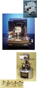
Figure 1. Digital Instruments Dimension 3100 AFM (top) and scanner head with Application Module (inset); and MultiMode AFM shown with Application Module ready head (inset). Four Application Modules support a wide range of advanced AFM scanning techniques
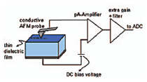
Figure 2. Schematic representation of the Tunneling-AFM (TUNA) and Conductive AFM (CAFM) setup.
Applications
Applications include, but are not limited to, failure analysis of semiconductor and data storage devices, two-dimensional carrier profiling of semiconductor devices, and conductivity studies of dielectric, metallic, polymer, organics, and semiconductor films. This application note discusses the techniques and a few of these many applications in greater detail.
Conductive AFM
CAFM is a powerful current measuring technique for mapping variations in electrical conductivity of materials (figure 3). CAFM can be applied to materials with medium conductivity (1pA to 1£gA). The CAFM application module can be operated in either imaging or spectroscopy mode. In the imaging mode, images of the electrical current are obtained, while in the spectroscopy mode one can collect current-voltage (I-V) or current-force (I-Z) spectra.
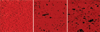
Figure 3. CAFM images map the conductivity of HfO2 as deposited (left) and post-anneal at 700C (middle) and 800C (right). These maps allows visualizing, and quantifying the size and distribution of weak spots in the dielectric. Darker color means higher current through the tip, indicating higher conductivity, and thus the weaker spots in the dielectric. Weak spots emerge and proliferate upon annealing, more at the higher anneal temperature. 500nm scans courtesy Jasmin Petry, IMEC, Belgium.
In the imaging mode, an electrically conductive probe is scanned over the sample surface in contact mode as a feedback loop keeps the deflection of the cantilever constant while local height of the sample is measured. During scanning, the user can apply a DC bias between the tip and the sample. A low-noise linear current amplifier senses the resulting current passing through the sample as the topography image is simultaneously obtained (see figure 2). The observed current can be used as a measure for the local conductivity or electrical integrity of the sample under study.
In addition to the imaging mode, CAFMalso measures local current voltage (I-V) or current-force (I-Z) spectra using the spectroscopy mode. In order to obtain I-V spectra, the imaging scan is stopped and the tip is held in a fixed location while the sample bias is ramped up or down. The resulting current through the sample is plotted versus the applied bias (figure 3a). User-selectable parameters include start and end voltage of the ramp, ramp direction, ramp rate, and delay times between individual ramps. The software can either record a single spectrum or average over multiple spectra. For some measurements, it is desirable to limit the current passing through the sample. In this case, the software provides the user with a ¡§trigger¡¨ option, which stops the voltage ramp as soon as the user selected current value is reached. In order to obtain I-Z spectra, the sample bias is kept constant, while the scanner is moved in the Z-direction, similar to the measurement of force-displacement curves. The resulting current through the sample is plotted versus the Z-position of the scanner. Again, several parameters allow the user to perform and control specific I-Z ramping experiments.
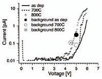
Figure 3a. CAFM Spectroscopy: Current versus Voltage (IV) plots with AFM tip positioned on weak spots of thin film (HfO2). (Averages from different locations) reveal background leakage current dropped with annealing, and average current at a given voltage increased after annealing, with increase annealing temperature.
An I-Z spectrum is displayed in figure 4. Here the CAFM module was used to study the current on a conductive polymer sample as a function of the applied force, or cantilever deflection. The electrical current, sensed by the CAFM module, is monitored while performing a standard force displacement ramping cycle. The current spectrum displays the details of the change in conductivity for the point contact as the probe makes contact with the sample and the force is increased.
Figure 4. Force-displacement (top) and I-Z spectrum (bottom) measured simultaneously with the CAFM module.
CAFM can be applied in many research and manufacturing areas for the analysis of a wide range of materials. It can also be used to localize and image electrical defects in semiconductor and data storage devices. In addition, CAFM can be applied to characterize conductive polymers and other materials with non-uniform conductivity, such as semimetals, semiconductor materials, conductive organic materials, nanotubes and others.
Tunneling AFM
TUNA measures ultra-low currents on low-conductivity samples. As with CAFM, a DC bias is applied between the sample and the conductive tip as the tip is scanning the sample in contact mode. A linear current amplifier with a range of 60 fA to 120 pA senses the resulting current passing through the sample. In this way, the sample¡¦s topography and current are measured simultaneously, enabling direct correlation of a sample location with its electrical properties. The noise level of the TUNA module (typ. 50 fA) allows one to perform extremely sensitive current measurements. In addition, the TUNA module also allows local measurement of current-voltage spectra on the sample.
The TUNA technique is especially useful for evaluation of thin dielectric films such as gate oxides (often SiO2) in transistors. In TUNA the current tunneling from the tip through the dielectric film strongly depends on film thickness, leakage paths (possibly caused by defects) and charge traps. All of these may significantly affect the properties and the integrity of the whole film, thus compromising an entire device¡¦s performance.
TUNA can be applied in many research or manufacturing areas and on a wide range of materials. It can be used to study the thickness uniformity or interface roughness of thin dielectric films, such as gate oxides. It can also be applied to localize and image electrical defects in semiconductor or data storage devices. In addition, TUNA can be used for the study of conductive polymers or organics, and other low-conductive materials (such as semimetals, semiconductor materials, etc.). Some typical examples follow.
Characterization Of Thin Silicon Oxide (SiO2) Films
One of the most demanding steps in the manufacturing of semiconductor devices is the gate dielectric. The thin dielectrics films (often SiO2 or high-k dielectrics) are used as gate oxides in field effect transistors and as tunnelling oxides and dielectrics for memory capacitors like dynamic random access memory (DRAM) and electrically erasable and programmable read only memory (EEPROM) devices. A structurally and electrically homogeneous oxide is of primary importance in order to comply with the requirements for reliability and long-term stability of the gate and tunneling oxides. Otherwise, degradation and breakdown lead to early device failure. Even variation of oxide thickness in the angstrom range can have a large impact on the electrical behavior of the transistor and memory devices. With decreasing oxide thickness this problem becomes much more severe. Surface and interface roughness result in increasing oxide fields and enhance leakage currents and Fowler-Nordheim tunneling, leading to fast degradation and limiting the scaling of oxides for metal-oxide-semiconductor (MOS) devices.
Conventional measurement techniques¡Xmacroscopic current voltage (I-V) and capacitance-voltage (C-V) spectroscopy, emission microscopy (EM), and transmission electron microscopy (TEM)¡Xare inadequate for locating and measuring the degree of oxide thinning. These methods either lack the required resolution or measure only structural (not electrical) information. TUNA on the other hand, provides the spatial resolution and sensitivity required to map effective thickness variations of thin dielectric films. A bias voltage, applied between sample and probe, gives rise to a tunneling current (hence the name Tunneling AFM) that strongly depends on the local electrical properties, i.e., the effective electrical thickness of the oxide. The conductive probe, the oxide film under investigation, and the semiconductor substrate form a local MOS structure. Generally, the current (often Fowler-Nordheim) increases exponentially with a linear change in film thickness, thus providing a very sensitive technique to monitor thickness variations.
Figure 5 shows a series of TUNA current images taken at different bias voltages on the bare surface of the oxide film. One can clearly observe the increase in current upon increasing the bias voltage. The current data taken at the highest voltage (9V) shows localized high-current spots in the scanned area, indicating electrical breakdown of the oxide film in these locations.
Figure 5. TUNA current measurements taken on a 5nm thick SiO2 gate oxide at increasing sample bias voltages from left to right: (top) 6V, 7V, (bottom) 8V, and 9V. 0.5£gm scans.
Specialized software also permits the measurement of I-V spectra in a single location on the sample surface. Figure 6 shows a typical I-V spectrum measured on the 5nm thick gate oxide, obtained by ramping the bias voltage from 0V to 2V. The spectrum shows the exponential dependence of the current on the applied bias voltage. TUNA can also be employed to monitor weak spots and inhomogeneities of thin dielectric films or oxides. Structural defects on the surface, as well as structural and electrical inhomogeneities within the oxide (e.g., SiO2) and at the interface to the substrate (e.g., Si), can be investigated.
Figure 6. I-V spectrum taken on a 5nm thick gate oxide. The spectrum was recorded while ramping the bias from the start voltage (0V) to the end voltage (2V) forward, and then back.
Figure 7 shows the topography and simultaneously obtained tunneling current image (at constant sample bias) at the transition from a field oxide to a 40nm thick gate oxide. The topography image shows (from left to right) the gate oxide, the interface region, and the field oxide. At the edge between the two regions an increased Fowler-Nordheim tunneling current is measured. This indicates local structural thinning of the gate oxide during the fabrication of the field oxide, which serves as an insulating area between adjacent active regions.
Figure 7. Topography (left) and simultaneously-obtained tunneling current image (right) at the transition from a field oxide to a 40nm thick gate oxide. At the transition the tunneling current is increased, which indicates thinning of the silicon oxide. 1£gm scans, 0.5 pA current scale. Image courtesy A. Olbrich, Infineon, Munich, Germany.
In figure 8, topography and tunnelling current images of an 8.5nm thick tunnel oxide for an EEPROM device are displayed. The tunnel oxide (SiO2) is enclosed by a thicker field oxide to the left and right. The data was obtained at a sample bias of 10V. Whereas the field oxide is too thick to show any measurable current at the given sample bias, the tunnel oxide shows inhomogeneities in current density, which indicates variations in the effective oxide thickness.
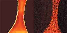
Figure 8. Topography (left) and tunnelling (right) current images of an 8.5nm thick tunnel oxide (SiO2) measured at a sample bias of 10V. 2£gm scans, 200 fA current scale. Image courtesy A. Olbrich, Infineon, Munich, Germany.
Imaging of Ultrathin Aluminium Oxide (Al2O3) Films
As an alternative to traditional nonvolatile memory devices, magnetic random access memories (MRAMs) are being investigated and developed. MRAMs operate based on the tunneling magneto-resistive (TMR) effect, and their essential part is a metal-insulator-metal (MIM) tunnel junction. Successful operation of these structures requires a chemically homogeneous (free of impurities) insulating barrier, as well as minimal fluctuations of the barrier thickness. Therefore it is important to spatially resolve the tunnel barrier and relate it to the macroscopic tunnel magnetoresistance. While conventional transmission electron microscopy (TEM) and x-ray photoelectron spectroscopy (XPS) studies provide global information on the atomic organization, surface-interface structure, and chemical composition, these techniques give incomplete information on the tunnel barrier quality at the atomic scale because they average over depth and surface. To date, TUNA is the only method that allows characterization of the local electrical properties of these films with very high lateral resolution. Figure 9 shows the topography and the tunneling current image of a 1.2nm thick Al2O3 layer, which lends itself as a very good insulator for MRAMs due to its large band gap (about 8 eV).
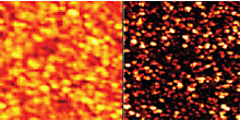
Figure 9. Topography (left) and tunnelling current (right) images taken on a 1.2nm thin aluminum oxide (Al2O3) film at a sample bias voltage of 0.14V. 500nm scans, 5 pA current range. Data courtesy A. Olbrich, Infineon, Munich, Germany.
Local variations in effective electrical thickness result in elevated currents - up to several orders of magnitude. It is noticeable that most often, areas with increased tunneling current seem to correspond with topographically elevated features.
Imaging of Defects Embedded in Silicon Oxide (SiO2) Films
An important application of TUNA is the localization and identification of electrical defects in thin dielectric films. In figure 10, a thin SiO2 film was embedded with a controlled amount of quantum dots, which can be viewed as small electrical defects. The small dots could not be observed when using standard SPM topography, but clearly show up in the TUNA current data. Upon increasing the bias voltage from 1V to 5V, more dots appear in the TUNA current images. This can be related to the size of the defects and the depth of the defects underneath the top surface. This example illustrates the possibility of using the TUNA technique to image and localize subsurface electrical defects, as well as to measure the defect size and density.
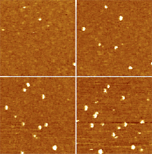
Figure 10. Sequence of TUNA images obtained on a SiO2 film with embedded defects. The sample bias voltage was from left to right: (top) 1V, 2V, (bottom) 3V, and 5V. 1£gm scan, 1 pA current scale. Samples courtesy S. Madhukar, Motorola, Austin, Texas.
Imaging of Diamond-Like Carbon (DLC) Films In Data Storage
A different application for TUNA can be found in the characterization of thin dielectric films used in the data-storage industry. A continuous effort is aimed at improving the performance and reliability of magneto-resistive (MR) read/write heads and disc media. For protection against corrosion and wear, the discs and heads are commonly coated with a thin non-conductive DLC film. TUNA can be used to determine the quality of these films. When applying a bias to the disc or head, the tunneling current is an excellent indicator of leakage paths, small inhomogeneities or defects (electrical contaminants, short circuits, DLC thinning, etc.) in the DLC coating.
Figure 11 shows the tunneling current images of two MR-heads with uniform coating. The topography image shows little detail of the MR head, whereas the TUNA current data looks through the DLC film and shows the different (metallic) regions of the MR head revealing defective coating. The tunneling current images clearly shows weak spots in the coating of the defective MR head. The application of TUNA on magnetic disc media, covered with a thin DLC film, is illustrated in figure 12. The topographic and TUNA current data are displayed for two samples, with a different DLC-coating thickness. The left image displays the data obtained on a disc with a thin DLC film. The TUNA current data vary between about 0 and 20 pA and show a strong spatial variation correlating with the polishing scratches present on the discs. The right image displays the data obtained on a disc with a slightly thicker DLC coating.
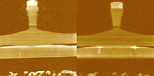
Figure 11. Tunneling current scans (left) measured on a magneto-resistive read/write head covered with a thin diamond-like carbon (DLC) film. Tunneling current image (right) of a similar head with defective DLC coating. 20£gm scans. Samples courtesy T. Ahmed, Seagate, Minneapolis, Minnesota.
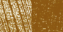
Figure 12. Tunneling current scans measured on two magnetic disc media covered with a thin (left) and slightly thicker (right.) DLC film. 0.5£gm scans, 20 pA current scale. Sample courtesy J. Leigh, Seagate, Fremont, California.
The average tunneling current is much lower, corresponding to the change in film thickness. Also, the correlation to the surface morphology is much less pronounced. This example illustrates how the TUNA technique can successfully assist in optimizing the thickness, composition and processing conditions of the DLC films.
Imaging of Thin Ferroelectric and Piezoelectric Films
Another important group of materials for applications in both MEMS and microelectronics are piezoelectric and ferroelectric materials. Of particular interest is BST (BaXSr1-XTiO3), which serves as a high-epsilon dielectric in volatile memory devices (DRAM) and PZT (PbZrXTi1-XO3), which may be used in ferroelectric memory devices. These oxides are polycrystalline, and so far the correlation between microscopic structure and their electrical properties are not well understood. Again, TUNA can be a useful technique to analyse local properties of these films. Enhanced current flow is noticeable along the grain boundaries, whereas less current is observed on individual grains. This behavior can, for example, explain the undesired leakage current of the ferroelectric capacitors fabricated with this type of film.
The TUNA data obtained on a 500nm thick BaTiO3 layer, is displayed in figure 13. A higher current is observed at some of the grain boundaries, as well as along some longer lines. One of these crack-like lines is displayed in the current image. The presence of these high-leakage current lines may be explained by stress phenomena in the imaged film. This effect is only observed in the TUNA current data.
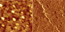
Figure 13. Topography (left) and tunneling current (right) images of a thin BaTiO3 ferroelectric film. 2£gm scan, 2 pA current scale. Sample courtesy H. Ruda, University of Toronto, Canada.
TUNA and CAFM Combined Imaging Of Conductive Polymers
In addition to the previously described inorganic materials, TUNA has also proven to be very useful for organic materials like conductive polymers. The data displayed in figure 14 was obtained using low spring constant probes on a 100nm thick polyphenylene vinylene layer (PPV) on top of a 200nm thick poly-aniline (PANI) layer. The PPV is a light-emitting polymer, which is spin-cast on top of a conductive buffer layer (PANI) to facilitate the transport of charge carriers. This particular sample had the PPV layer partially peeled off to enable measurements of the PANI layer underneath. The PPV part of the sample is slightly higher and visible on the left in the topography image. The corresponding current image clearly shows a uniformly lower conductivity of the PPV compared to the inhomogeneous PANI buffer layer.
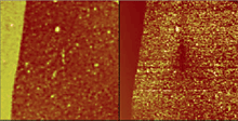
Figure 14. Topography (left) and TUNA current (right) images of a 100nm PPV layer on a conductive PANI layer. The sample bias voltage was -6V. 50£gm scan. Sample courtesy C. Zhang, Uniax, Goleta, California.
A second conductive polymer example, with higher spatial resolution, is shown in figure 15. The CAFM technique was used to map the spatial variation of the conductivity in a thin poly-analine film deposited on an Indium Tin Oxide substrate. The relatively high conductivity of this sample required the use of the CAFM module, instead of the TUNA module. The observed currents varied between 0 and 200 pA. The CAFM image shows the high conductivity of the large areas covered with PANI, and a slightly lower conductivity for the smaller, isolated spots covered with PANI. The substrate appears as a poorly conductive region. The low spring constant probe employed allows scanning at very low contact forces, hence minimizing the deformation or wear of these relatively soft samples.
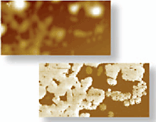
Figure 15. Topography (top) and CAFM current (bottom) images of a poly-analine film on an indium tin oxide substrate. 2£gm x 1£gm scan, 200 pA current scale. Sample courtesy S. Rane, University of Chicago, Illinois.
Scanning Capacitance Microscopy
The continuing miniaturization of semiconductor devices has created a serious challenge for traditional materials analysis techniques, such as secondary ion mass spectrometry (SIMS), spreading resistance profiling (SRP), and capacitance voltage (C-V) measurements. While the accuracy, reliability, and improved capabilities of these instruments provide the basis for current materials characterization data, their one-dimensional limitation, inability to measure sub-0.1-mm features, and limited characterization repertoire have increased the value of scanning probe techniques. SCM was one of the first SPM techniques to find its way into the advanced semiconductor analysis world. SCM instruments can show the carrier concentration profiles in two dimensions in actual semiconductor devices, as well as the relationship of these profiles to critical device structures. This capability makes the SCM module useful in the development, manufacturing, testing, and failure analysis of semiconductor devices.
In SCM, the metalized probe forms a metal-insulator-semiconductor (MIS) capacitor with the semiconductor sample. An AC bias applied between the scanning contact AFM tip and the sample generates capacitance variations, which are monitored using a gigahertz resonant capacitance sensor. This system has been shown to be sensitive to variations smaller than attofarads (<10¡V18 F). The capacitance variation (dC/dV) is a measure of the local carrier concentration density and type (n-type or p-type), and can therefore be used for high-resolution two-dimensional carrier profiling.
2-D Carrier Profiling In Semiconductor Device Structures
One of the most important applications of SCM is two-dimensional carrier profiling of semiconductor device structures. Both silicon and compound semiconductors are of great interest. Two-dimensional dopant profiling is a high priority on the International Technology Roadmap for Semiconductors, and it is expected to become an enabling technology for next-generation device manufacturing. SCM provides the spatial resolution (about 10¡V20nm), and dynamic range (1015¡V1020 atoms/cm3) to answer these needs.
Figure 16 shows the topography (left) and SCM dC/dV (right) images obtained simultaneously on a cross sectioned transistor from a Pentium II processor. The topography shows the gate region with the two spacers (bright areas), but shows no details of the carrier profiles. The SCM dC/dV image shows the differently doped areas of the transistor: source, drain (both high- and low-dose implants are visible) and gate. The SCM image can be used to extract valuable information such as the effective gate length, junction depth, or details on the lateral and vertical extension of the doped regions. With the exception of SSRM, this crucial information is not accessible through any other technique.
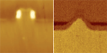
Figure 16. Topography (left) and SCM dC/dV (right) of a crosssectioned transistor of a Pentium II processor. 1.25£gm scan.
In addition to imaging, SCM can also be used to measure dC/dV versus V curves in selected positions on the sample. In figure 17, the DC sample bias is ramped between two user selected values, and the SCM sensor output (dC/dV) is monitored and plotted. The top curve was measured on an n-type sample, while the bottom curve was measured on a p-type sample. As expected, different types result in a different sign of the dC/dV signal, and different dopant levels result in a different intensity of the dC/dV signal.
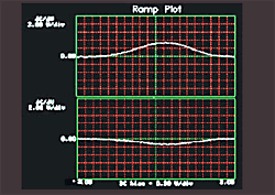
Figure 17. dC/dV versus V curves measured with SCM on two different locations of a sample: n-type, 2x10¹⁷ atoms/cm3 (top curve) and p-type, 3x10¹⁹ atoms/cm3 (bottom curve).
Figure 18 illustrates topography (left), amplitude (middle), and capacitance (right) of top metal and dielectric etched layer of a Silicon DRAM cell.
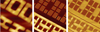
Figure 18. Height or topography (left), Capacitance (SCM) dC/dV amplitude (middle), and Capacitance (SCM) dC/dV phase (right) images of a conventional Silicon DRAM cell. Top metal and dielectric layers were etched to expose Silicon. The SCM dC/dV phase image differentiates ptype (bright color) and n-type (dark color) doped areas. npn and pnp transistors in DRAM cell are then clearly visualized, allowing extraction of critical parameters, e.g., effective gate length, and visualizing defects. The SCM dC/dV amplitude image shows relative magnitude of dopant concentration: bright color means larger depletion capacitance, and therefore, lower doped areas (e.g., well implant areas).
Figure 19 illustrates capacitance (left) and topography (right) of an ion-implanted Silicon structure consisting of an n-type implant into a p-type substrate.
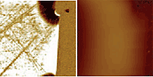
Figure 19. Capacitance (SCM) dC/dV phase (left) and height/topography (right) images of an ion-implanted Silicon structure consisting of an n-type implant (dark areas) into a p-type substrate. An additional (shallower) p-type implant can be observed. The structure has been cross-sectioned by standard polishing techniques.
SCM is also a very valuable tool for failure analysis on semiconductor devices. The SCM technique allows visualization of whether a particular implantation is present, whether it is the correct type (n or p), the expected dimensions (both in-depth and lateral), and other characteristics. A typical failure analysis example is shown in figure 20. A cross-sectional surface was made through a number of devices, including one known to have bad electrical device characteristics. The SCM image of a good device is shown in the top image; the SCM image of the corresponding area of the bad device is shown in the bottom image. The bottom image indicates that the two implanted regions (i.e. the bright areas: n-type implant and n-type well implant) are touching, whereas they should be separated from each other. This ¡§short circuit¡¨ resulted in a very high leakage current of this particular device.
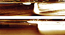
Figure 20. SCM image of a good (top) and failed (bottom) silicon device. The bottom image displays a short circuit between the two doped regions. 8£gm x 2£gm scan.
Ferroelectric Films
Ferroelectric thin films are very attractive for their possible applications in nonvolatile memories and microelectromechanical devices (MEMS). The decrease in size (down to tens of nanometers) of these devices requires an appropriate description of the material properties and processes in ferroelectric films. For example, it is fundamental to investigate whether ferroelectric structures with nanometer dimensions still exhibit ferroelectric and piezoelectric properties, and to study how these properties are affected by the overall size. SCM is a possible technique for these studies. For example, SCM provides a method for measuring the sign of the C-V slope for the ferroelectric sample and, hence, the domain or polarization state in the thin film. SCM has been used to image and manipulate the domain structure in a thin Pb1.0(Nb0.04Zr0.28Ti0.68)O3 (PNZT) ferroelectric film. On an area of 25x25£gm, the tip was scanned with a DC sample bias voltage of -12V and subsequently smaller areas were written with DC sample bias voltages of opposite polarity. A small AC bias voltage was used to image the polarized regions, i.e., to study the magnitude and sign of the slope of the C-V curve at zero DC bias. Figure 21 shows the SCM image on the right and the corresponding AFM topography image on the left. The dark and light contrast regions indicate oppositely polarized regions, where the dC/dV signal is of high strength but opposite sign.
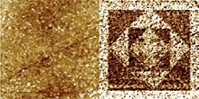
Figure 21. Topographic (left) and SCM dC/dV image (right) of a PNZT ferroelectric film. Dark and bright areas correspond to oppositely polarized regions. The different polarization regions were written using the SCM at different scan sizes and sample bias voltages prior to this SCM scan. 25£gm scan. Sample courtesy Ch. Ganpul and M. Ramesh, University of Maryland.
In addition, SCM can also measure the polarization (or C-V) curves of small ferroelectric capacitors, or even of single ferroelectric grains. This is impossible with conventional probing techniques. Figure 22 illustrates topography (left) and capacitance (right) of FerroElectric thin film on top of platinum electrode. Whereas figure 23 shows approximately the same areas as in above images, but now with a 5V DC applied between tip and sample. The DC voltage changes the polarization such that all grains have the same polarization state. And lastly, figure 24 shows hysteresis typical of a ferroelectric domain on a single grain with localized capacitance spectroscopy versus applied DC bias (V).
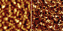
Figure 22. Height/topography (left) and capacitance (SCM) dC/dV phase images (right) of FerroElectric thin film on top of platinum electrode. Height image shows granular structure of thin film with 20-100nm sized grains. The SCM dC/dV phase image shows individual grains¡¦ polarization states; it is obtained by applying a small amplitude AC voltage between tip and sample that modulates the capacitance at the same frequency (DC voltage is kept at 0V not to change the polarization state by the presence of AFM tip). Ferroelectric polarization state is determined by charge measurement performed in SCM. The resolution of the SCM technique allows one to observe variations within single grains.
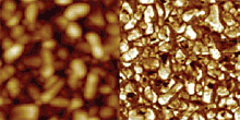
Figure 23. Approximately the same areas as in above images, but now with a 5V DC applied between tip and sample. The DC voltage changes the polarization such that all grains have the same polarization state.
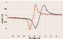
Figure 24. Localized capacitance spectroscopy (exclusive to SCM) dC/dV versus applied DC bias (V) on a single grain shows the hysteresis typical of a ferroelectric domain. The data can be integrated once to obtain a Capacitance versus DC bias curve, and twice to obtain a relative Polarization versus DC bias curve.
Scanning Spreading Resistance Microscopy
Like SCM, SSRM is often used to measure dopant profiling in semiconductors, but it does so by quantifying electrical conductivity or resistivity. SSRM provides two dimensional information on the electrical conductivity or resistivity of the sample under study. Veeco has developed and patented this technique in collaboration with IMEC, Belgium. In SSRM, an electrically conductive probe is used to measure the sample¡¦s local resistivity. When the probe is scanned in contact mode over regions with different resistivity r, the electrical resistance R formed by the probe sample contact will vary proportionally. If the contact is assumed to be circular and of Ohmic nature, the relation between R and r is given by the basic spreading resistance formula: R = r / 4r, whereby r is the radius of the contact. Since the resistance can vary over several orders of magnitude, a logarithmic current amplifier is used for SSRM. The logamp has a current range of seven orders of magnitude from 10 pA up to 0.1 mA. A major application of SSRM is the measurement of the two-dimensional distribution of electrical carriers inside semiconductor structures.
2-D Carrier Profiling in Semiconductor Device Structures
While the probe is scanned across the cross-section of the semiconductor device, the electrical resistance is measured between the conductive tip and a large current collecting back contact. When the applied force exceeds a certain threshold force, the measured resistance is dominated by the spreading resistance. On Si structures, high forces (typically, a few £gN) are required in order to penetrate the native oxide and to establish a stable electrical contact. Since standard AFM probes deform at these high forces, doped diamond or diamond-coated silicon probes are employed. The extreme hardness, high Young¡¦s modulus, and the electrical conductivity obtained through doping make diamond particularly suitable for use as SSRM tip coating material.
In figure 25, analysis has been performed on a Si DMOS transistor structure. The transistor structure was cross-sectioned to expose the differently doped regions, and then polished using standard polishing techniques. The topographical image (left) shows quite clearly the Al-contact (black region), the underlying oxide (brown) and the polysilicon and underlying gate oxide. The SSRM resistance image (right) shows the electrically active regions. The different colors reflect different levels of resistivity: dark indicates highly conductive regions, and bright indicates low conductivity. Clearly observable are the highly doped n+-substrate (black); the lower doped n-epilayer (dark brown); the p+-body (which appears as highly resistive), the n+-implant (black), the metal and the oxide regions, as well as the highly conductive polysilicon material. Junction positions correspond to the sharp transition between the various color levels.
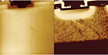
Figure 25. Topography (left) and resistance (right) scans of a cross-sectioned Si DMOS transistor. 12£gm scan courtesy IMEC, Belgium.
Figure 26 illustrates an SSRM image of a cross-sectioned capacitor featuring a metal think film area with dielectric between them. SSRM images are often complementary to SCM images, as SCM images give no signal on dielectrics and metals, whereas SSRM shows a big contrast between the two.
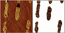
Figure 26. SSRM height and resistance images of cross sectioned capacitor. The capacitor has metal thin film area with dielectric between them. If there were leakage paths between the different electrical contacts, the resistance image would show them (none found in this image).
In a second example (figure 27), SSRM imaging was performed on a silicon MOSFET with a gate length of 0.25£gm. The image (left) shows the differently doped regions ¡V source, drain, and gate ¡V as highly conductive areas (dark), dielectric and substrate as low-conductivity areas, as well as the intermediately conductive area. The source and drain junctions are observed as thin, bright lines of low conductivity. A section made through the source region of the transistor is also shown in figure 27 (right). The section shows from left to right: the dielectric top layer, source implant (p-type), junction peak, well (n-type), and substrate. The junction depth can easily be extracted from this section as the distance between the junction peak and the dielectric top layer, and is found to be 184nm.
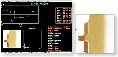
Figure 27. SSRM resistance scan of a cross-sectioned 0.25£gm silicon MOSFET transistor. 2£gm scan courtesy IMEC, Belgium.
In addition to silicon, compound semiconductors are also of great interest. LEDs, photodetectors, and diode lasers are only a few of the many devices fabricated from III-V and II-VI semiconductors. Knowledge of the two-dimensional distribution of conductivity (the electrical-active dopant atoms in particular) is important for process development and monitoring. For compound semiconductors, sample preparation is minimal; simple cleaving provides the best surface on complex samples, and allows imaging of critical device properties after only minutes of sample preparation. Metal and metal-coated silicon tips prove to be sufficiently rigid for stable and reproducible SSRM measurements. For good signal to noise ratio, a relatively high bias voltage (several volts) in combination with a medium probe pressure (sub- £gN) is required. An example of the high-resolution carrier density profiling available with SSRM can be seen in the cross-sectioned InP-based heterostructure shown in figure 28.
Figure 28. Topography (left) and SSRM resistance (right) scan of an InP-based heterostructure. 7£gm scans. Sample courtesy of M. Geva, Lucent Technologies, Breinigsville, PA.
The resistance image shows the different regions of the heterostructure: alternating Zn-doped p-type and S-doped n-type layers with different thickness values. The image reveals the two-dimensional nature of the layers toward the mesa area. This example demonstrates SSRM analytical power in two-dimensional imaging of carrier distributions in compound semiconductor structures, and in particular, for the analysis of InP hetero-structures, an area that is gaining high interest.
Conductivity Mapping of Nonsemiconductor Materials
SSRM can also be used for studying the electrical properties of nonsemiconductor materials. This includes applications for metals, semimetals, conductive polymers, and other intermediately conductive materials. For optimum performance, different materials often require different probe material and force set points. In the example in figure 29, a Cu film is imaged. The granular structure of the film is clearly observed in the topographic data. The SSRM resistance data show that the resistivity of the grains is higher towards the edges, as compared to the center of the grains. Note that the average grain size is 30nm, and the spatial resolution is on the order of 5nm.
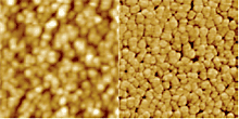
Figure 29. Topography (left) and SSRM resistance (right) scan of a granular metal film. 500nm scans.
Summary
The Digital Instruments MultiMode, Dimension 3100/5000 and CP-II SPMs set the standard for ultra high resolution topographical profiling and mapping of sample hardness, elasticity, friction, adhesion and magnetic or electrical field strength. Now, with the addition of add-on application modules for CAFM, TUNA, SCM, and SSRM, these industry-leading instruments can be enhanced to map nanometer-scale resolution on a wide range of additional properties on various materials including low- and midstrength electrical currents, resistance, and capacitance. These enabling technologies, which are already being used successfully in both industry and science, promise to play ever increasing roles in future process optimization and scientific research.
.png)
This information has been sourced, reviewed and adapted from materials provided by Veeco.
For more information on this source, please visit Veeco.