The fabrication of high-brightness light emitting diodes (HB-LEDs) is done on sapphire wafers. The substrate is patterned with tiny structures, enhancing the light extraction efficiency of finished devices. Critical issues such as refractive index mismatch and crystal dislocations are also solved using patterned sapphire substrates (PSS).
The Zeta-PSS package offers quick characterization of substrate bump features. A single scan is capable of measuring pitch, height and width. All types of substrate bump recipes are available including dome-shaped, cone-shaped, flat topped or photo-resist.
Figure 1 shows some example scans on a Zeta Optical Profiler system.
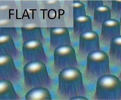
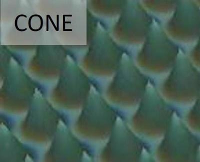
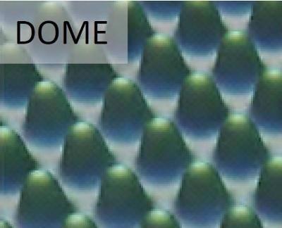
Figure 1. Example scans on a Zeta Optical Profiler system.
Automated Feature Analysis
Figure 2 shows a cross sectional line with a surface profile, statistics for width, height, pitch and feature spacing in the field of view as well as two-dimensional and fully-adjustable three-dimensional view of PSS bumps.
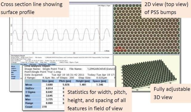
Figure 2. Cross section analysis and associated characteristics of PSS bumps measured with Zeta Optical Profiler.
Salient Features
The features of the Zeta-PSS package are:
- The Zeta Optical Profiler takes a scan (70 X 90 μm) in seconds of a large area.
- Zeta 3D software enables a one-page analysis report that includes two-dimension and three-dimensional images, a cross section and statistical analysis of all features in the field of view.
- A large number of results are saved in a spreadsheet text format.
- Automated X-Y stage and multi-site recipes enable characterization of the entire wafer.
- Manual load system for R&D and automated XY stage for production.
- Vacuum chucks for wafers of different sizes.
- Vibration and Environmental noise isolation package.
- Piezo-stage for 2-nm height resolution.
- True color 3D imaging enable review of defects such as scratches or missing bumps.
Zeta 3D Software analyzes standard two-dimensional or three-dimensional wafer images for general surface characterization:
- Step height.
- Surface roughness.
- Feature size, diameter, area and volume.
- Wafer bow.
- 3D surface visualization in true color.
- Statistics.
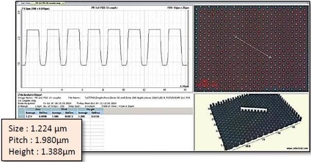
Figure 4. Optional Piezo Z stage provides 2-nm, Z-height resolution and 3s repeatability of less than ±15 nm*.
Figure 5. Zeta 3D Optical Profiler with piezo-stage and 2” wafer chuck.

This information has been sourced, reviewed and adapted from materials provided by KLA Corporation.
For more information on this source, please visit KLA Corporation.