Feb 24 2015
Renishaw, a world leader in metrology and spectroscopy technologies, has teamed up with Bruker’s Nano Surfaces Division to host a series of workshops on TERS (tip-enhanced Raman spectroscopy) and co-localised AFM-Raman (atomic force microscopy - Raman spectroscopy).
The latest workshop took place at the end of January at Renishaw’s headquarters at New Mills, Wotton-under-Edge, UK. Other workshops are planned to take place throughout the world.
An audience of spectroscopists and microscopists recently attended the joint workshop designed to illustrate how to make TERS more accessible to users. Four talks on the techniques, backed by various applications examples, preceded an afternoon of demonstrations of the latest instrumentation given by applications specialists from co-hosts, Renishaw and Bruker Nano Surfaces Division.
The first invited talk came from Aravind Vijayaraghavan from the National Graphene Centre in Manchester. Graphene and other similar 2D materials are well suited to characterisation by both Raman and AFM. Dr Vijayaraghavan’s research looks at the integration of nano-carbons with plasmonic and photonic systems. In particular, he pointed out the use of Raman to follow the strain processes in graphene and how polarisation could be used to assist in his measurement of the efficiency of plasmonic antennae.
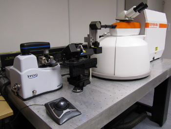
Next was a well-delivered description of the recent advances in the integration of AFM and Raman by Tim Batten (Renishaw). This talk stressed the value of combining the two techniques, with Raman providing information on sample chemistry to complement the nanoscale physical property measurements delivered by AFM.
The second of the invited talks was given by Claus Burkhardt from the Natural & Medical Sciences Institute at the University of Tübingen, Germany. Dr Burkhardt leads a team developing new implants to aid the blind and deaf. The Institute has successfully developed an intelligent retina implant and is now working on a cochlea implant. Central to these microimplants are the arrays of electrodes. In the encapsulation process, AFM, SEM (scanning electron microscopy) and Raman are used to check successive deposition and removal processes.
The talks were completed with more applications examples from Mickael Febvre (Bruker Nano). Particular attention was given to the choice of different tips for TERS applications. The choice of experimental parameters for measurements can greatly affect resultant imaging and spectra. For example, tip height when in feedback and polarisation dependency.