A research team headed by physicists from the University of Arizona has discovered that boron nitride, a non-conducting material but structurally identical with graphene, can control the flow of electrons in graphene.
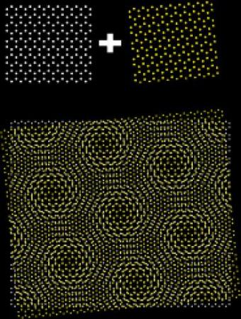 When a sheet of graphene sits atop a sheet of boron nitride at an angle, a secondary hexagonal pattern emerges that determines how electrons flow across the sample.
In 2011, the research team found that boron nitride can be used as a mounting surface for single-atom-thick graphene sheets. The team also discovered that boron nitride not only offers mechanical support but also enhances the nanomaterial’s electronic properties by stabilizing electronic charge fluctuations.
The research team’s latest results, reported in Nature Physics, paves the way for manipulating the flow of electrons in graphene. Brian LeRoy, principal investigator of the study, stated that it is difficult to stop the electron flow in graphene due to relativistic quantum mechanical effects, which make the electrons to behave unusually at atomic scales. This makes graphene not suitable for fabricating electronic devices like transistors.
Now, the team has found that when graphene sheets are mounted over boron nitride sheets at certain angles, some of the electrons are prevented from traversing the other side of the nanomaterial by creating a hexagonal superlattice structure, thus opening the door to effectively control the flow of electrons. The team also discovered that the electron flow is completely stopped at one point at a specific angle.
Matthew Yankowitz, one of the researchers, explained that the effect relies on the hexagonal pattern’s size. The pattern is purely an electronic effect caused by the two materials’ structure and how they have assembled. However, hitherto the research team has not been able to control the end-up orientation of the two materials relative to each other during their integration. Hence, the team tested several samples and investigated their structures using a scanning tunneling microscope.
Yankowitz informed that samples that have very small hexagonal pattern are not suitable, and only 10% to 20% of samples have demonstrated the desired effect. Graphene microelectronics may be possible someday if this method is automated.
Source: http://www.arizona.edu