Apr 22 2015
 High-mobility polysilicon layer was directly formed on paper by coating liquid silicon, which was annealed by pulsed laser-light. (CREDIT: R. Ishihara, M. Trifunovic/TUDelft)
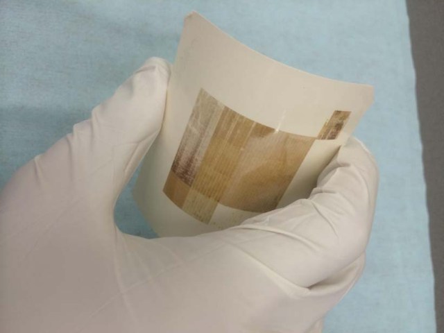
Researchers from Delft University of Technology, in the Netherlands have formulated a fabrication method which allows silicon in polycrystalline form, as found in circuitry, to be manufactured directly on a substrate using liquid silicon ink along with a single laser pulse. This new method has the potential to beat all other recently created ultra-thin substitutes.
Researchers have been focused on finding an alternative to silicon in their pursuit of developing advanced micro-electronic transistors. Plenty of research has been conducted on using varied organic and metal-oxide ink materials to create fully flexible electronic circuitry. However these materials do not possess silicon’s positive electronic properties although they do possess excellent “printability."
Printing silicon ink onto substrates has been in existence for awhile; however a thermal annealing step at 350°C was required, which was a highly extreme temperature to create flexible surfaces. This unappealing step can be skipped in this new fabrication method as liquid silicon can be directly transformed into polysilicon.
"It was very simple," said Ryoichi Ishihara, the professor who led the research team at Delft University of Technology, with collaborators at the Japan Advanced Institute of Science and Technology in Ishikawa, Japan.
"We coated liquid polysilane directly on paper by doctor-blading, or skimming it by a blade directly in an oxygen-free environment. Then we annealed the layer with an excimer-laser [a conventional tool used for manufacturing smartphone displays]. And it worked," Ishihara said.
The time taken for the laser blast was hardly a few tens of nanoseconds, therefore having no effect on the paper. While analyzing its conductive performance, Ishihara’s team discovered that thin-film transistors made from the laser-printed layer displayed high mobilities matching those of traditional poly-silicon conductors.
This printing method can find immediate application in wearable electronics because it allows economical production of fast, low-power and flexible transistors. Going forward
Ishihara’s team will focus on enhancing the production method of thin-film transistors by including extra non-silicon layers, which subsequently will pave the way for numerous probable applications.
"The process can be expanded to biomedical sensor and solar-cell areas," Ishihara said, "and will also realize stretchable -- and even edible -- electronics!"
The research findings will appear in Applied Physics Letters, from AIP Publishing.