Apr 22 2015
Researchers have successfully created a new three-atomic-layer-thick semiconducting material. The novel material has electronic properties better than conventional semiconductors. The material’s two nano-engineered configurations have exhibited improved light response.
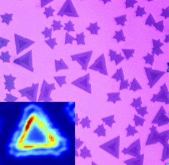 Optical microscope image of triangular-shaped metal-diselenide monolayer hetero-structures. The central portion containing molybdenum atoms appears darker than the outer portion with tungsten atoms. Inset is a photoluminescence intensity map showing that the linear junction region along the triangular interface produces enhanced light emission (red region). Image courtesy of University of Washington
The new ultra-thin semiconducting material comprises a heavy metal atom layer sandwiched between two selenium layers, representing an “atomic sandwich” configuration. The quasi-two dimensional material shows exotic properties at junctions.
Under light exposure, the material absorbs photons and consequently electrons are excited. However, the excited electrons continue to be coherently coupled, in a unique fashion, with the charge “hole” leaving behind by them.
When two “atomic sandwiches” are stacked up, coupled excited charge states are generated across the planar interface with the alignment of the magnetic direction or “spin state” aligned for a large population of electrons.
A companion result by the same research team showed an approach of matching up the edge of one metal layer with the edge of a second, different metal layer, which is a linear boundary or “hetero-junction” instead of the planar boundary.
Charge polarization and engineered electron spin, in addition to transport along or across the interface, might be possible as confirmed by the improved photoluminescence signals at these positions.
It is possible to engineer layered materials at the atomic limit, where electrons are confined to two dimensions, into electronic structures exhibiting exotic magnetic, optical and electronic properties.
The new structures can be used to test the theories of low dimensional materials physics. By optically controlling magnetic order and electron charge, flexible, transparent computation devices and new methods of solar energy conversion can be developed.
The DOE Office of Science, Basic Energy Sciences provided the primary support. Some researchers received support from the Hong Kong Research Grant Council, the Croucher Foundation, the Science City Research Alliance and the University of Washington Clean Energy Institute. Some students received support from graduate student fellowships and doctoral training grants (NSF, EPSRC, HEFCE, and Cottrell Scholar Award).