A team of researchers at the Oak Ridge National Laboratory, Department of Energy, has integrated a new synthesis process with standard electron-beam lithography methods to create complex and scalable arrays of semiconductor heterojunctions in random patterns within a nanometer-thick semiconductor crystal. This unique process depends on converting patterned areas of a single-layer crystal into another layer of crystal. The study has been published in Nature Communications.
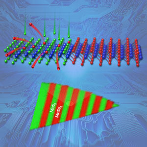 Complex, scalable arrays of semiconductor heterojunctions—promising building blocks for future electronics—were formed within a two-dimensional crystalline monolayer of molybdenum deselenide by converting lithographically exposed regions to molybdenum disulfide using pulsed laser deposition of sulfur atoms. Sulfur atoms (green) replaced selenium atoms (red) in lithographically exposed regions (top) as shown by Raman spectroscopic mapping (bottom). Image credit: Oak Ridge National Laboratory, U.S. Dept. of Energy
Transistors are the electronic building blocks of microchip-enabled devices such as computers and smartphones. These transistors are developed by integrating metals, semiconductors, and insulators. The current generation of transistors is very small, measuring just 10nm wide, and are produced from 3D crystals. However, a novel technology utilizes 2D crystals that measure just 1nm in thickness to allow extremely thin electronics.
To that end, researchers across the globe are testing 2D crystals produced from standard layered materials to restrict transport of electrons within two dimensions. Scientists recently discovered several ways to lithographically pattern graphene, a one-layer carbon atoms, into ribbon-like wires insulated with an identical layer of boron nitride. However, to date, synthesis and processing techniques have not been developed to lithographically pattern heterojunctions between two types of semiconductors inside a nanometer-thick layer to produce transistors.
In the latest technique, the research team initially synthesized nanometer-thick layers of crystals of molybdenum diselenide on suitable substrates and then used traditional lithography methods to deposit protective patterns of silicon oxide. Next, the exposed areas of the crystals were bombarded with a laser-produced beam of sulfur atoms. The selenium atoms in the crystals were substituted by these sulfur atoms, thus forming molybdenum disulfide with a similar crystal structure. Both semiconductor crystals created sharp junctions, which are the preferred building blocks of ultrathin electronics.
We can literally make any kind of pattern that we want.
Masoud Mahjouri-Samani, who co-headed the research
Geohegan is the head of ORNL’s Nanomaterials Synthesis and Functional Assembly Group at the Center for Nanophase Materials Sciences and also the chief investigator of a Department of Energy basic science project devoted to controlled synthesis and growth mechanisms of nanomaterials.
Mahjouri-Samani stated that a countless number of 2D building blocks containing many patterns can be produced simultaneously. The research will look at developing different types of patterns on both the top and bottom of a sheet and even layering sheets with different patterns.
The development of a scalable, easily implemented process to lithographically pattern and easily form lateral semiconducting heterojunctions within two-dimensional crystals fulfills a critical need for ‘building blocks’ to enable next-generation ultrathin devices for applications ranging from flexible consumer electronics to solar energy.
Geohegan
“We chose pulsed laser deposition of sulfur because of the digital control it gives you over the flux of the material that comes to the surface,” said Mahjouri-Samani. “You can basically make any kind of intermediate alloy. You can just replace, say, 20 percent of the selenium with sulfur, or 30 percent, or 50 percent.”
Geohegan added, “Pulsed laser deposition also lets the kinetic energy of the sulfur atoms be tuned, allowing you to explore a wider range of processing conditions.”
If the amount of sulfur to selenium in the crystal is controlled properly, the bandgap of the semiconductors can be adjusted accordingly, a key feature that establishes both optical and electronic properties. In order to fabricate electroluminescent displays and other optoelectronic devices, microchip fabricators combine semiconductors having different bandgaps, for instance the bandgap of molybdenum disulfide is comparatively higher than the bandgap of molybdenum diselenide.
When voltage is applied to a crystal comprising both semiconductors, both holes and electrons shift from molybdenum disulfide into molybdenum diselenide and again combine to generate light at the molybdenum diselenide’s bandgap. Due to this aspect, multi-color light can be produced by fabricating the bandgaps of monolayer systems. This approach would also allow for other applications such as sensors and transistors, added Mahjouri-Samani.
The research group is planning to see whether their pulsed laser vaporization and conversion technique will equally work with atoms, other than selenium and sulfur atoms.
We’re trying to make more complex systems in a 2D plane—integrate more ingredients, put in different building blocks—because at the end of the day, a complete working device needs different semiconductors and metals and insulators.
Mahjouri-Samani
In order to gain a better insight into the process of changing a single, nanometer-thick crystal into another crystal, the team applied ORNL’s powerful electron microscopy, particularly atomic-resolution Z-contrast scanning transmission electron microscopy developed at the lab and can now be accessed by researchers across the globe through the Center for Nanophase Materials Sciences.
Visiting scientist Leonardo Basile and Electron microscopists Andrew Lupini used this method to capture hexagonal arrangement of separate columns of atoms in the molybdenum disulfide and molybdenum diselenide crystals measuring nanometer-thick.
We could directly distinguish between sulfur and selenium atoms by their intensities in the image. These images and electron energy loss spectroscopy allowed the team to characterize the semiconductor heterojunction with atomic precision.
Lupini
The paper is titled “Patterned Arrays of Lateral Heterojunctions within Monolayer Two-Dimensional Semiconductors.” The U.S. Department of Energy, Office of Science funded the study
Part of the study was performed at the Center for Nanophase Materials Sciences, a DOE Office of Science User Facility at ORNL. The National Secretariat of Higher Education, Science, Technology and Innovation of Ecuador supported Basile’s research.
References