Feb 3 2017
The majority of electronic devices that surround us have semiconductors at its core. The proper functioning of semiconductor devices depends upon its internally generated electric fields. The development of next-generation electronics would be possible if these fields could be measured on the nanoscale. However, current methods have been limited to measurements of the electric field at the surface of the semiconductor.
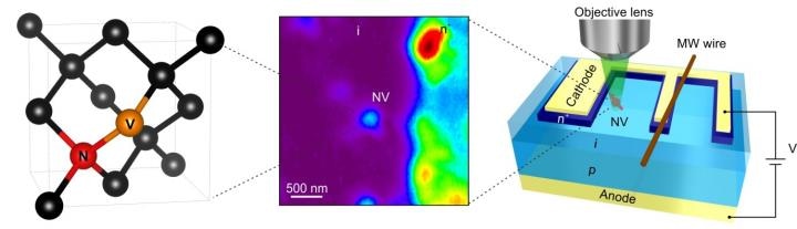 Left: Schematic of the structure of the NV center. Middle: Confocal fluorescence image of a single NV center in the device. Right: Schematic of the measurement configuration. (CREDIT - Tokyo Institute of Technology)
A group of Takayuki Iwasaki, Mutsuko Hatano and colleagues at the Tokyo Institute of Technology, the Japan Science and Technology Agency (JST) and Toshiharu Makino at the National Institute of Advanced Industrial Science and Technology (AIST) has formulated a new technique for sensing internal electric fields within operating semiconductor devices. The method takes advantage of the response of an artificially initiated single electron spin to variations in its surrounding electric field, and enabled the group to explore a semiconductor diode exposed to bias voltages of up to 150 V.
Iwasaki and team used their technique to diamond, a so-called wide-band-gap semiconductor in which the electric fields can turn out to be very strong – an attribute essential for low-loss electronic applications. Diamond has the benefit that it smoothly accommodates nitrogen-vacancy (NV) centers, a type of point defect that occurs when two neighboring carbon atoms are eliminated from the diamond lattice and one of them is substituted by a nitrogen atom. NV centers can be regularly formed in diamond using ion implantation. A close by electric field affects the energy state of a NV center, which in turn can be probed by a technique called optically detected magnetic resonance (ODMR).
The researchers initially fabricated a diamond p-i-n diode (an intrinsic diamond layer sandwiched between a hole-doped and electron layer) embedded with NV centers. Subsequently, they localized an NV center in the bulk of the i-layer, many hundreds of nanometers away from the interface, and captured its ODMR spectrum for boosting bias voltages. Using these spectra, values for the electric field could be acquired with theoretical formulas. Then the experimental values were compared with numerical results acquired with a device simulator and established to be in excellent agreement -- verifying the potential capabilities of NV centers as local electric-field sensors.
Iwasaki and team clarify that the experimentally verified value for the electric field around a specified NV center is fundamentally the field's component perpendicular to the path of the NV center – arranged along one of four probable directions in the diamond lattice. They explained that a standard matrix of implanted NV centers should facilitate reconstructing the electric field with a spatial resolution of approximately 10 nm by incorporating with super-resolution methods, which is promising for researching more intricate devices in future studies.
The researchers also mention that electric-field sensing is not only applicable for electronic gadgets, but also for electrochemical uses: the success of electrochemical reactions occurring between a semiconductor and a solution relies on the former's interior electric field. Additionally, Iwasaki and team note that their method need not be limited to NV centers in diamond: related single-electron-spin structures are present in other semiconductors such as silicon carbide.
Background
Wide-band-gap semiconductors
Semiconducting materials feature a band gap, which refers to an energy range in which no accessible energy levels exist. In order for a semiconductor to conduct, it is essential for electrons to acquire adequate energy to overcome the band gap; monitoring electronic transitions across the band gap develops the basis of semiconducting device action.
A band gap of the order of 1 electron volt (eV) is present in typical semiconductors like silicon or gallium arsenide. A larger band gap, in which values as high as 3-5 eV are not uncommon, is present in wide-band-gap semiconductors, like diamond or silicon carbide.
Wide-band-gap semiconductors can work at temperatures beyond 300 ℃ because of their large band gap. They are also capable of sustaining high voltages and currents. These properties enable the wide-band-gap semiconductors to have several applications, including high-power components, alternative-energy devices, transducers and light-emitting diodes. Characterization of wide-band-gap devices in operation will help in further development of these and various other future applications. The method proposed by Iwasaki and colleagues for measuring the electric field produced in a wide-band-gap semiconductor subject to large bias voltages is thus considered to be a significant step forward.
Nitrogen–vacancy centers
Diamond is made up of carbon atoms set on a lattice where each atom comprises of four neighbors developing a tetrahedron. The diamond lattice is subject to defects, and one such defect is the nitrogen–vacancy (NV) center, which can be considered as resulting from replacing a carbon atom with a nitrogen atom and removing one neighboring carbon atom. The energy level of an NV center is present in the band gap of diamond, however it is sensitive to its local environment. The so-called nuclear hyperfine structure of an NV center in particular depends on its surrounding electric field. This dependence is theoretically well understood, and was explored by Iwasaki and co-workers. Together, they obtained values for the local electric field by detecting changes in an NV center's hyperfine structure. One significant advantage of this approach is that it permits controlling the field within the material and not just at the surface, for which methods had been previously developed.
Optically-detected magnetic resonance
Iwasaki and colleagues used optically detected magnetic resonance (ODMR) for exploring the nuclear hyperfine structure of an NV center in the bulk of the diamond-based device. Irradiating the sample with laser light resulted in the NV center becoming optically excited after which it was possible to record the magnetic resonance spectrum. The ODMR resonance is made to split by an electric field, and a measure for the electric field is provided by the experimentally detected split width.