Apr 4 2017
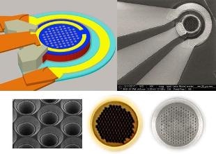 Tapered black holes in silicon, about 1 micrometer in size, can trap photons and act as a photodetector for high-speed data connections. (Saif Islam, UC Davis)
A silicon wafer has tiny “black holes” that act as a new form of photodetector for potentially moving more data across a data center or around the world, in a less expensive manner. Electrical engineers at the University of California, Davis, and a Silicon Valley startup, based at Los Altos, California, called W&WSens Devices Inc., have developed this technology, which is reported in the April 3 issue of Nature Photonics.
We’re trying to take advantage of silicon for something silicon cannot usually do. If we don’t need to add nonsilicon components and can monolithically integrate with electronics into a single silicon chip, the receivers become much cheaper.
Saif Islam, Professor of Electrical and Computer Engineering, UC Davis
Tapered holes present in a silicon wafer are used by the new photodetector for diverting photons sideways. This allows maintaining the efficiency of a thicker layer and the speed of thin-layer silicon. So far, an experimental photodetector and solar cell have been built by Islam’s team by employing the new technology. Data conversion, from optical to electronics, is done by the photodetector at the rate of 20 GB per second (or 25 billion bits per second, over 200 times faster than the cable modem), and achieves a quantum efficiency of 50%. The data conversion is the fastest ever reported for a device of this efficiency.
Data centers need fast connections
Data centers powering the internet “cloud” have witnessed growth, which has generated a demand for devices capable of very quickly moving large quantities of data, over distances ranging from a few yards to hundreds of yards. According to Islam, such connections could also be employed for high-speed home connections.
Computer engineers employ fiber-optic cables, transmitting data as pulses of light, to quickly move large amounts of data either across a data center or across the world. However, at the receiving end, a photodetector should convert these signals to electronic pulses. Silicon can be used as a photodetector — incoming photons produce a flow of electrons, with a tradeoff between efficiency and speed. In order to capture most of the photons the silicon must be thick, however this slows down the process. To work faster, the silicon can be made thinner, but this has a cost of losing many photons.
Materials such as indium phosphide and gallium arsenide have been used by circuit designers to fabricate high-efficiency, high-speed photodetectors. At the same scale and wavelength, gallium arsenide is about 10 times more efficient than silicon. However, this material cannot be monolithically integrated with silicon electronics, and is also substantially more expensive.
Tapered holes as light traps
Experiments were conducted by Islam’s team to find out ways to increase silicon’s efficiency by the addition of tiny columns or pillars, and then holes to the silicon wafer. The team, after experimenting for two years, finalized on a pattern of holes tapering toward the bottom.
We came up with a technology that bends the incoming light laterally through thin silicon.
Saif Islam, Professor of Electrical and Computer Engineering, UC Davis
The working principle is that photons, after entering the holes, are drawn sideways into the silicon. The wafer measures about 2 μm in thickness. Since the photons travel sideways, they move through 30 to 40 μm of silicon, similar to the ripple of waves produced in a water pond if a pebble is dropped into it.
According to Islam, the holes-based device can possibly work with a broader range of wavelengths of light in comparison to the existing technology.
Additional authors on the paper are: at UC Davis, Yang Gao, Hilal Cansizoglu, Kazim Polat, Soroush Ghandiparsi, Ahmet Kaya, Hasina Mamtaz, Ahmed Mayet, Yinan Wang, Xinzhi Zhang and Aly Elrefaie; Toshishige Yamada at UC Santa Cruz and W&WSens Devices Inc.; Ekaterina Ponizovskaya Devine and Shih-Yuan Wang, W&WSens Devices Inc.
The S.P. Wang and S.Y. Wang Partnership, the U.S. National Science Foundation, and the Army Research Office supported the work.