Jul 27 2017
A new hybrid integrated platform has been developed by Physicists from the ARC Centre of Excellence for Ultrahigh bandwidth Devices for Optical Systems (CUDOS). This new platform has the potential to be a more advanced alternative to standard integrated circuits that are presently developed by the semiconductor industry.
The Researchers proved that their approach is mass manufacturable, establishing the possibility to incorporate the platform into electronic equipment, such as computers and smartphones, that are used every day. For the end user, this new technical development means that it could result in faster internet on their next-generation electronic devices.
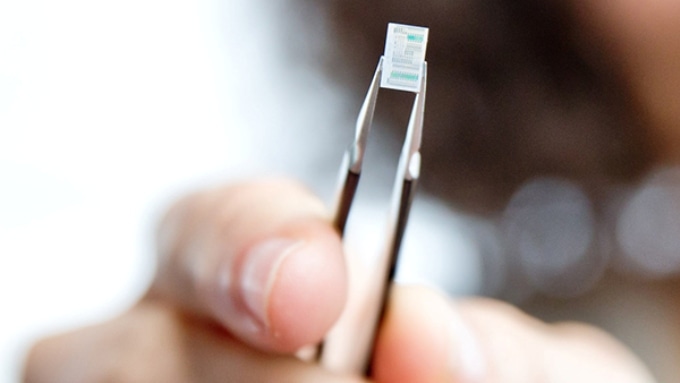 The new device is smaller than a thumbnail with a size of 0.1 x 4mm, and could be integrated into everyday electronic devices like smartphones. Credit: CUDOS
Chips, also known as integrated circuits, are utilized in everyday electronic equipment such as computers and mobile phones. It refers to a set of electronic circuits on a single small flat piece of semiconductor material, usually silicon. However, this material has a few limitations when it comes to data processing.
Researchers are currently developing optical circuits produced from chalcogenide glass in order to overcome these restrictions and enhance data processing. This superior type of glass is utilized for ultrafast telecommunication networks in order to transmit information at the speed of light.
Incorporating these glass optical circuits into silicon chips may result in a much improved communications system capable of processing data a hundred times faster. It is possible to combine these two materials?
The answer indeed is yes. The CUDOS research group headed by PhD Candidate Blair Morrison and Senior Researcher Dr Alvaro Casas Bedoya collaborated with Physicists in the University of Sydney’s Australian Institute for Nanoscale Science and Technology (AINST), the Australian National University (ANU) and RMIT University in order to produce compact, mass manufacturable optical circuits with improved functionalities by incorporating non-linear glasses with silicon-based material.
In the last few years the group at the University of Sydney has repeatedly demonstrated exciting functionalities, such as broadband microwave devices that can enhance radar, using these novel chalcogenide glasses. Now we have shown it is possible to combine this material with the current industry standard platform for photonic integration, silicon.
Blair Morrison, the University of Sydney CUDOS node
“We integrated a novel nonlinear glass into an industrially scalable CMOS compatible platform. We maintained the key advantages of both the silicon and the glass, and made a functional and efficient ultra-compact optical circuit,” stated Dr Alvaro Casas Bedoya who is the lead Photonics Nanofabrication Manager for CUDOS.
“A wealth of new opportunities will be created, and this takes us one step closer to moving our research from the lab into industrial applications,” said Blair Morrison.
CUDOS Director and ARC Laureate Fellow Professor Benjamin Eggleton from the University of Sydney stated that this new approach will someday permit the industry to miniaturize the photonics functionalities from devices that are similar in size like that of a smartphone or a laptop or even smaller, enabling deployment in real world applications.
This is exciting, because this is a platform which is more compatible with existing semiconductor manufacturing and will allow us to integrate multiple functionalities on a single silicon chip, with active and passive components, such as detectors and modulators, required for advanced applications.
Professor Benjamin Eggleton from the University of Sydney, CUDOS Director and ARC Laureate Fellow
The multi-university research team studied the whole manufacturing process: Silicon wafers used in the fabrication of these devices were obtained from a semiconductor foundry in Belgium, a devoted facility in ANU’s Laser Physics Centre for the glass deposition, lithography in the RMIT University’s School of Engineering. The devices are then characterized and tested in the University of Sydney’s AINST.
The CUDOS Researchers showcased the potential of this new approach by further demonstrating a compact novel laser based on the light-sound interactions, for the very first time in an integrated optical circuit.
The breakthrough here is this realization that we can actually interface, we can integrate that glass onto silicon and we can interface from silicon to the glass very efficiently – we can harness the best of both worlds.
Professor Benjamin Eggleton from the University of Sydney, CUDOS Director and ARC Laureate Fellow
The research has been published in the July 26th edition of Optica.
Professor Susan Pond, the Director of AINST, highlighted that this project is one of AINST flagship activities dealing with harnessing interactions between photons and phonon at the nanoscale. In this study, fundamental research in light matter interactions at the nanoscale is linked with an end user perspective and powerful coupling to industry.