A research team at Penn State has developed a two-dimensional (2D) bilayer material by integrating one-to-two-atom-thick graphene layer with a hexagonal boron nitride (hBN) layer having a thickness of few to several hundred atoms for fabricating wafer-scale transistors with improved performance.
 A team of Penn State researchers has developed field effect transistors using graphene and hexagonal boron nitride on a 75mm wafer, a significant step toward graphene-based electronics. (Credit: Joshua Robinson)
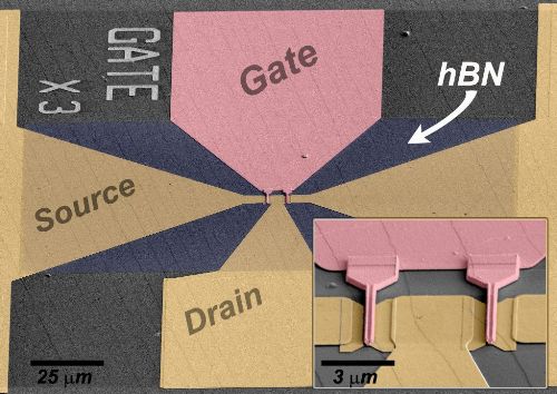
The research work has been reported online in the ACS Nano journal. The research team used a prior method devised in its laboratory to fabricate a superior-quality, large-area, homogenous epitaxial graphene layer ideal for use in high frequency applications. In the process, hydrogen atoms bonded to the graphene to passivate dangling bonds, resulting in quasi-freestanding epitaxial graphene, a smoothened and flattened graphene film.
The researchers then used a chemical vapor deposition system to grow the hBN over a transition metal substrate. The hBN was then made to release from the substrate using one of the transfer processes. The released hBN was then applied over the graphene on a 75-mm wafer. This is the first time an epitaxial graphene was integrated with hBN at an industrial scale.
Joshua Robinson, one of the researchers, stated that this latest work demonstrates a 2-3x performance improvement when compared to the researchers’ previous work with epitaxial graphene that improved the performance of graphene-based transistors by two to three times, indicating the realization of graphene electronics.
The researchers believe to develop graphene-based ICs and other high-performance devices ideal for industrial-scale production on 100-mm wafers in the near future. A novel material that can improve performance and is compatible with existing processing technologies is essential in today’s competitive microchip industry. The new bilayer material developed by the Penn State is one such material that can fabricate functional graphene field effect transistors for use in high frequency electronic and optoelectronic devices.
Source: http://www.mri.psu.edu