Feb 7 2023Reviewed by Alex Smith
A team at the University of Michigan has now reduced the thickness of ferroelectric semiconductors to only 5 nm, or around 50 atoms, making them suitable for bridging current computers with future devices.
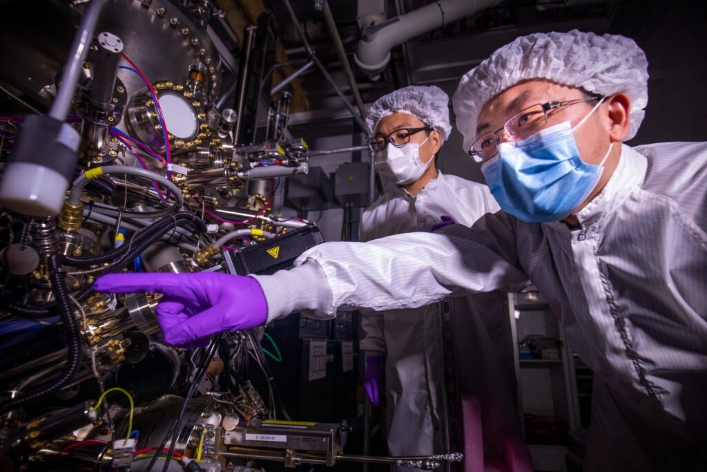 Research scientists Ding Wang (left) and Ping Wang (right) discuss the growth behavior of the ferroelectric semiconductor deposited using the molecular beam epitaxy system that is visible on the left. The semiconductor could make computing more efficient, enhance AI and enable quantum computing. Image Credit: Robert Coelius.
As a result, it will be possible to combine ferroelectric technologies with traditional computer and smartphone components, enhancing artificial intelligence and sensor capabilities.
They could also make battery-less gadgets possible, which are essential for the Internet of Things (IoT), which, among other things, enables smart homes, detects issues with industrial systems, and warns people about potential dangers.
The study published in Applied Physics Letters was chosen as the editor’s pick.
This will allow the realization of ultra-efficient, ultra-low-power, fully integrated devices with mainstream semiconductors. This will be very important for future AI and IoT-related devices.
Zetian Mi, Study Co-Corresponding Author and Professor, Electrical and Computer Engineering, University of Michigan
Ferroelectric semiconductors are distinctive from other types because they can maintain an electrical polarization, which is the equivalent of magnetism on an electrical level. They can, however, change which end is positive and which is negative, unlike a fridge magnet.
This capability can be employed in a variety of applications, including energy harvesting and the detection of light and sound vibrations.
Mi added, “These ferroelectric devices could be self-powered. They can harvest ambient energy, which is very exciting.”
Additionally, they provide a distinct method of processing and storing information, both classical and quantum. For instance, in computing, the two electrical polarization states can represent one and zero. This method of computation can also mimic the neural connections that allow the brain to process information and store memories.
This type of architecture, sometimes referred to as neuromorphic computing, is excellent for enabling AI algorithms that use neural networks to analyze data.
The capacitors in RAM must be continually powered; otherwise, the data they contain would be lost. Electrical polarization takes less energy to retain energy and could outlive an SSD. This type of memory could be packed more densely, boosting capacity, while also being more resistant to severe temperatures, high humidity, and radiation.
In a semiconductor constructed of aluminum nitride spiked with scandium, a metal frequently used to reinforce aluminum in performance bicycles and fighter planes, Mi’s team has previously observed ferroelectric activity.
However, they needed to be able to produce it in layers thinner than 10 nm, or around the thickness of 100 atoms, to employ it in modern computer equipment.
The team accomplished this using a process known as molecular beam epitaxy, which is the same method used to create the semiconductor crystals that power CD and DVD players’ lasers. They were able to create a crystal that was 5 nm thick—the tiniest scale ever—in a device that had definite steampunk characteristics.
They achieved this by carefully regulating each layer of atoms within the ferroelectric semiconductor and by reducing atom losses from the surface.
By reducing the thickness, we showed that there is a high possibility that we can reduce the operation voltage. This means we can reduce the size of the devices and reduce the power consumption during operation.
Ding Wang, Study First Author and Research Scientist, Electrical and Computer Engineering, University of Michigan
Additionally, due to the material’s unusual optical and acoustic properties, nanoscale manufacturing could pave the way for its use in quantum technologies by helping researchers better understand the fundamental properties of the material and determine the constraints of its performance at small sizes.
With this thinness, we can really explore the miniscule physics interactions. This will help us to develop future quantum systems and quantum devices.
Ping Wang, Research Scientist, Electrical and Computer Engineering, University of Michigan
Defense Advanced Research Projects Agency provided funding for the study.
The studies were carried out at the Michigan Center for Materials Characterization and the Lurie Nanofabrication Facility.
Journal Reference:
Wang, D., et al. (2023) Thickness scaling down to 5 nm of ferroelectric ScAlN on CMOS compatible molybdenum grown by molecular beam epitaxy. Applied Physics Letters. doi:10.1063/5.0136265.
Source: http://umich.edu/