Electron backscatter diffraction (EBSD) is an SEM-based method that provides crystallographic data regarding the microstructure of a sample. This method involves interaction between an electron beam and a slanted crystalline sample, and the diffracted electrons create a pattern that can be identified with a fluorescent screen.
The diffraction pattern can be used to measure the crystal orientation, characterize grain boundaries, differentiate between crystallographically different phases, characterize grain boundaries, and provide data regarding the local crystalline perfection.
When the beam of electrons is scanned in a grid across a polycrystalline specimen and the orientation of the crystal is determined at each point, the ensuing map shows the grain orientations, morphology, and boundaries. This information can also be utilized to reveal the desired crystal orientation in the sample. This way, a quantitative representation of the microstructure can be determined using the EBSD technique.
A well established accessory for the SEM, EBSD is used in a wide range of applications to aid in materials characterization, as illustrated in Table 1. This article describes how an EBSD system functions and provides relevant examples of the type of results that can be produced by EBSD.
Table 1. A summary of the different application areas and the typical types of measurement made using EBSD.
| Industries |
Materials |
Typical EBSD Measurements |
| Metals research and processing |
Metals, Alloys |
Grain size |
| Aerospace |
Intermetallics |
Grain boundary characterisation |
| Automotive |
Inclusions / precipitates / 2nd phases |
Global texture |
| Nuclear |
Ceramics |
Local texture |
| Microelectronics |
Thin Films |
CSL boundary charcterisation |
| Earth Science |
Solar Cells |
Recrystallised / deformed fractions |
| Academia |
Geological |
Substructure analysis |
| |
Semiconductors |
Phase identification |
| |
Superconductors |
Phase fractions / distributions |
| |
Ice |
Phase transformation |
| |
Metal / ceramic composites |
Fracture analysis |
| |
Bone, teeth |
Orientation & misorientation relationships between grains / phases |
Basics of EBSD
Principle System Components
Figure 1 shows a standard EBSD setup. It includes a crystalline sample slanted to 70o, using a pre-tilted holder or the SEM stage; a sensitive camera along with optics for visualizing the pattern formed on the phosphor screen; a phosphor screen; an insertion mechanism, which precisely controls the detector’s position; electronics to control the SEM; a PC to control the EBSD experiments; and optional forescatter diodes (FSD).
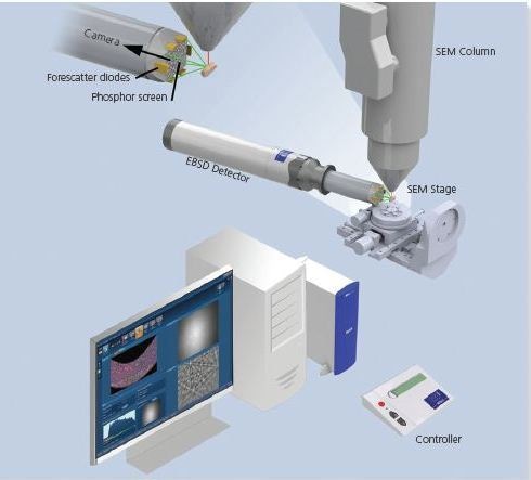
Figure 1. The principal components of an EBSD system
Pattern Formation and Detection
The model shown below explains the principle aspects of pattern formation and detection for the EBSD study. When an electron beam is focused at a point of interest on a slanted crystalline sample, the atoms in the material disperse a part of the electrons, with minimal loss of energy to create a divergent source of electrons near to the sample surface. Some of these electrons incident on atomic planes at angles that satsify the Bragg equation:
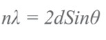
where λ is the wavelength of the electrons, n is an integer, θ the angle of incidence of the electrons on the diffracting plane, and d is the spacing of the diffracting plane.
When diffracted, these electrons create a group of paired large-angle cones, which match with each diffracting plane. The image thus formed on the phosphor screen includes typical Kikuchi bands, which are formed where the areas of enhanced electron intensity cross the screen, as shown in Figure 2.
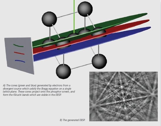
Figure 2. The formation of the electron backscattered diffraction pattern (EBSP).
Band Intensity
The mechanisms that promote the Kikuchi band intensities and profile shapes are quite complicated. As an estimation, the Kikuchi band intensity for the plane (hkl) is given by:
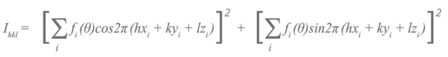
The diffraction pattern that is collected must be compared with a simulated pattern that was measured using the prior equation. This makes sure that only planes that generate visible Kikuchi bands are utilized while resolving the diffraction pattern.
The number of reflectors to use relies on the phases that are required by the system to differentiate between, and on the crystal symmetry of the phases.
Interpreting the Diffraction Pattern
The Kikuchi bands’ centre lines correspond to where the diffracting planes cross with the phosphor screen. Therefore, the Miller indices of the diffracting crystal plane indexes each Kikuchi band. The semi-angle of the diffracted cones of electrons is (90 - θ)o. This is a large angle for EBSD, and hence the Kikuchi bands approximate to straight lines.
Since the diffraction pattern is joined to the sample’s crystal structure, as the orientation of the crystal changes, the ensuing diffraction pattern also changes. The positions of the Kikuchi bands can thus be utilized to determine the orientation of the diffracting crystal, as illustrated in Figure 3.
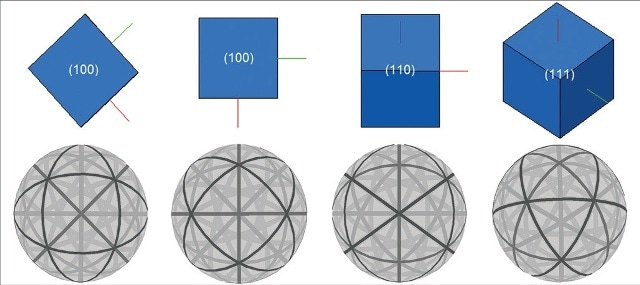
Figure 3. The spherical diffraction patterns generated by different orientations of a cubic structure.
Calibrating an EBSD System
In order to ensure that an EBSD system operates accurately, it should be calibrated first. The calibration of the EBSD system involves determining the pattern-centre position and the sample-to-screen distance on the phosphor screen.
A number of techniques are available that can be used for calibrating the EBSD system. The most preferred technique is to obtain diffraction patterns from the same point on a specimen with the detector positioned at different insertion positions, as shown in Figure 4.
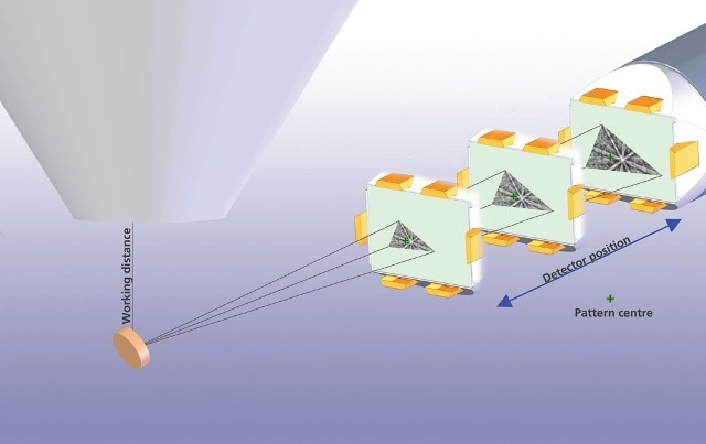
Figure 4. The pattern centre is found by correlating features on the EBSPs at different detector positions. The pattern centre is the zoom point on those EBSPs - the one point which does not move when the detector moves.
Basics of Automated Indexing
After the EBSD system has been calibrated, the diffraction patterns can be automatically indexed and the crystal orientation can be determined. The entire process is automatic and takes only a few milliseconds on a modern PC.
The Hough Transform
The Hough transform is used to locate the positions of the Kikuchi bands and changes the image from the EBSD camera into a representation in Hough space, by utilizing the following relation between the coordinates (ρ, θ) of the Hough space and the points (x, y) in the diffraction pattern:
ρ = x cosθ + y sinθ
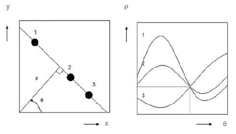
Figure 5. The Hough transform converts lines into points in Hough space.
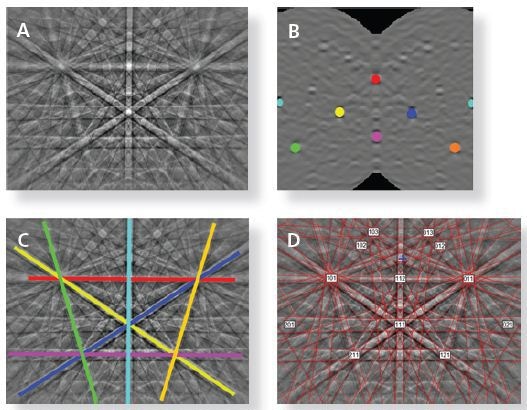
Figure 6. Finding the position of the Kikuchi bands in the diffraction pattern using the Hough transform.
A straight line seen in the image space (x, y) can be differentiated by ρ, and the perpendicular distance from the line to θ and origin and can be represented by one point (ρ, θ) in Hough space, as denoted in Figure 5. The Kikuchi bands materialize as bright peaks or regions in Hough space, which can be detected and utilized to measure the original positions of the band, as shown in Figure 6.
Conclusion
The EBSD is a SEM-based technique that provides crystallographic data routinely. This technique is employed in a variety of application areas, such as metals research and processing, automotive, aerospace, nuclear, earth science, academia, and microelectronics, to help in materials characterization.

This information has been sourced, reviewed and adapted from materials provided by Oxford Instruments NanoAnalysis.
For more information on this source, please visit Oxford Instruments NanoAnalysis.