Evident has introduced the MX63 and MX63L microscope systems that have been improved for high-quality inspections of wafers measuring as large as 300 mm, as well as circuit boards, flat panel displays, and other bulk samples.
The modular design of the microscopes allows users to select their preferred components to customize the system according to their application needs.
Such ergonomic and easy-to-use microscopes help boost throughput and, at the same time, keep inspectors comfortable while they do their work.
Integrated with the EVIDENT Stream image analysis software, users’ entire workflow, right from observation to report generation, can be streamlined.
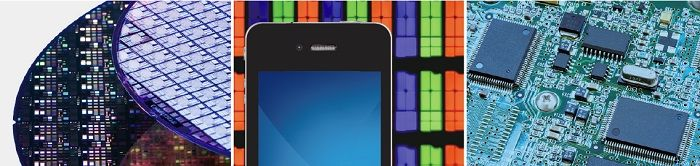
Image Credit: Evident Corporation - Industrial Microscopy
Functional
The MX63 and MX63L microscopes have been engineered to fulfill the safety and ergonomic needs of the electronics sector with added functionality to improve analysis abilities.
User-Friendly
Streamlined microscope settings make it relatively easy for users to make adjustments and recreate system settings.
Advanced Imaging Technology
The proven optics and excellent imaging technology from Evident enable consistent inspections and offer clear images.
Modular
Users can tailor their systems by using the components that suit their specific applications.
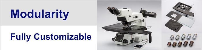
Image Credit: Evident Corporation - Industrial Microscopy
Application Image Gallery
The sophisticated image management capability offered by Evident shows what users really want to see.
Applications
The MX63 series is utilized in an array of reflected light microscopy applications. Such applications are an example of certain ways the microscope is employed for industrial inspections.
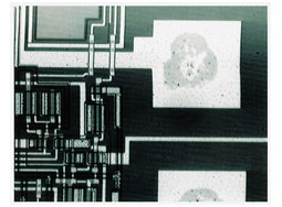
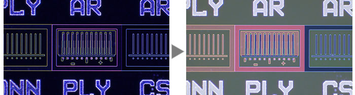
IR image of an electrode section. Image Credit: Evident Corporation - Industrial Microscopy
Infrared (IR) is utilized to search for defects within IC chips and other devices produced from silicon on glass.
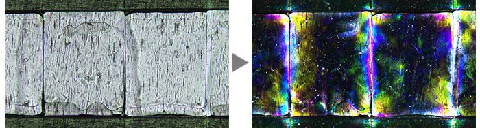
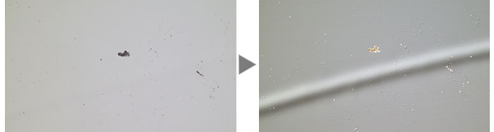
Film (Left: Brightfield/Right: Polarized light). Image Credit: Evident Corporation - Industrial Microscopy
Polarized light is utilized to unravel the texture of material and the condition of crystals. It is appropriate for inspecting LCD and wafer structures.
A hard disk (Left: Brightfield/Right: DIC). Image Credit: Evident Corporation - Industrial Microscopy
Users can use the differential interference contrast (DIC) to view samples that have minuscule height differences. DIC is perfect for inspecting samples that have extremely small height differences, like polished wafers, hard-disk media, and magnetic heads.
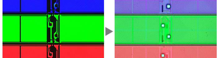
IC pattern on a semiconductor wafer (Left: Darkfield/Right: MIX (Brightfield + Darkfield)). Image Credit: Evident Corporation - Industrial Microscopy
Darkfield is used for inspecting samples that have mirrored surfaces, like wafers, or for identifying slight flaws or scratches on a sample. MIX illumination allows users to view both colors and patterns.
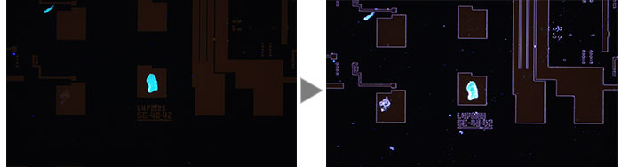
Photoresist residue on a semiconductor wafer (Left: Fluorescence/Right: MIX (Fluorescence + Darkfield)). Image Credit: Evident Corporation - Industrial Microscopy
Fluorescence is utilized for samples that produce light when illuminated with a specially designed filter cube. This method is used to identify photoresist residue and contamination. MIX illumination allows users to observe both the IC pattern and photoresist residue.
An LCD color filter (Left: Transmitted Light/Right: MIX (Transmitted Light + Brightfield)). Image Credit: Evident Corporation - Industrial Microscopy
This observation method is well-suited for transparent samples, like glass materials, plastics, and LCDs. MIX illumination allows users to view both the circuit pattern and filter color.