Introduction The physical properties of amorphous carbon (a-C) have been the subject of intense experimental and theoretical work [1-3]. Amorphous carbon is a disordered phase of carbon without long-range order containing carbon atoms mostly in graphite-like sp2 and diamond-like sp3 hybridization states, and its physical properties depend strongly on the sp2/sp3 ratio. There are many forms of sp2-bonded carbons with various degrees of graphitic ordering, ranging from microcrystalline graphite to glassy carbon. In this work, a-C thin films grown by electron-gun evaporation (EGE) are studied. There is a limited number of works using the EGE technique to grow a-C films, and we believe it is important to widen the knowledge in this direction. The main experimental parameter varied during growth was the source-substrate distance (SSD), and important changes in the physical properties: vibrational modes, dark conductivity and majority carrier concentration, are studied. The structural analysis shows that films have strong graphitic component and the behavior of the Raman modes features follows the graphite to nanocrystalline graphite route when SSD increases, in accordance with the description given by Ferrari and Robertson [1]. Experimental For the a-C and a-C:N films deposition by EGE, the electron-gun had a voltage of 6 kV and a current of 200 mA. Cleaned commercial glass slides and Si(100) single-crystal wafers were employed as substrates. The base pressure reached in the vacuum-chamber was 5 x 10⁻⁶ Torr, then, for a-C:N films ultrapure N2-gas was introduced up to 2 x 10⁻⁴ Torr, which was the working-pressure. Due to the infrared radiation emitted by the crucible, the temperature reached into the vacuum-chamber was 150ºC in average. For the SSD the values 10.5, 12.5, 15.5, 18.5 and 23.5 cm were chosen. A plausible assumption is the longer the SSD, the larger the N concentration in a-C films. The deposition time (TD) was 0.5 minutes for all the samples analyzed. Characterization of vibrational modes of samples was carried out through Raman spectroscopy, by using a Labram-Dilor micro-Raman apparatus with a He-Ne laser as the excitation source. The thickness was determined by utilizing a Dektak II profilometer. Dark conductivity was measured by employing the traditional two-point method using a conventional set-up. Carrier type (n-type) and concentration were determined by means of Hall effect measurements carried out in a home-made system. X-ray diffraction (XRD) patterns were registered using a Siemens D5000 diffractometer. All the above mentioned measurements were carried out at room temperature. Results and Discussion The thickness of the films was in the range 15-48 nm, the larger the SSD values, the smaller the thickness. XRD patterns indicate that the material is amorphous. In Figure 1, the Raman spectra of the films are displayed, for a-C samples the SSD values are: (a) 12.5 cm, (b) 15.5 cm, (c) 18.5 cm, (d) 20.5 cm; for the a-C:N films only for SSD values of (e) 15.5 cm and (f) 12.5 cm are shown. 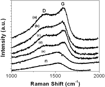
Figure 1. The Raman spectra of the films are displayed for a-C samples. The SSD values are: (a) 12.5 cm, (b) 15.5 cm, (c) 18.5 cm, (d) 20.5 cm; for the a-C:N films only the SSD values of (e) 15.5 cm and (f) 12.5 cm are shown. All the spectra of the a-C films are composed of two broad bands, one band named D at ~1380 cm-1, and the other named G at ~1590 cm-1. The a-C:N films exhibit a very attenuated D band at ~1345 cm-1 and a well defined red-shifted G band at ~1525 cm-1. The signals D (disorder) and G (graphitic) arise from the sp2 bonds only. Both the G and D modes correspond to bond stretching modes. The G mode is the stretching vibration of any pair of sp2 sites, whether in C = C chains or in aromatic rings. The D mode arises from a breathing mode of sp2 sites in rings not in chains. The broadening of the bands is due to the amorphous character, actually the short range ordering of the layers. The spectra were fitted with the Breit-Wigner-Fano function plus a Lorentzian curve [1], from here the position and the full width at half maximum (FWHM) of the G-band, and the intensities ratio (ID/IG) were determined. The plots of these data versus SSD are illustrated in Figure 2. 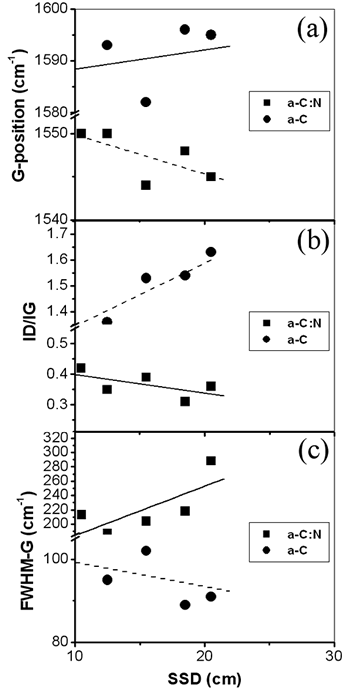
Figure 2. (a) G Raman band position, (b) ID/IG ratio of the intensities of D and G bands, and (c) FWHM of the G peak of the a-C and a-C:N thin films as a function of the SSD. For a-C films the G position increases in the interval 1582 – 1596 cm-1, the ID/IG ratio grows in the interval 1.36 – 1.63 and the FWHM decreases in the interval 89 – 102 cm-1 when SSD increases. The variation of the G position and the ID/IG ratio in these intervals closely follows the amorphization trajectory with 0% sp3 in the stage I of the Ferrari and Robertson Model (FRM) [1]. The average temperature in the vacuum-chamber due to the thermal radiation from the crucible is ~150°C. In our case, the larger the SSD, the lower the substrate temperature (Ts), in such a way that, by effect of different Ts values the average diameter (La) of the short-range clusters (grains) diminishes as SSD increases. It has been established that in the stage I of the FRM, ID/IG ∝ La-1 [1], this implies that ID/IG increases if SSD augments. Then, one can assure that as SSD increases the a-C films become more disordered with smaller nanocrystalline grains, and the material passes from a more graphitic state to a less graphitic state with an increasing content of rings as SSD rises. The FWHM decreases because the augments of the density of these rings. On the other hand, in a-C:N films the G position decreases in the interval 1544 – 1550 cm-1, ID/IG decreases in the interval 0.31 – 0.42 and the FWHM increases in the interval 187 - 288 when SSD augments. The behavior of these three parameters is completely opposite to the case of a-C films. The introduction of N favors the creation of sp3 sites, consequently, the amorphization trajectory can be located on the stage II of the FRM, where sp3 density runs from 0% to 20%, and where the G frecuency and the ID/IG ratio decrease. In the case of our films, as SSD increases the N-content increases, which in turn means that the density of sp3 sites rises. The FWHM increases because the material becomes most disordered, because the main disordered effect in stage II can be taken as the decreasing of the number of the ordered rings [1]. The dark conductivity (σ) of the films versus SSD is displayed in Figure 3. The variation of a-C films is located in the range (1.0 ± 0.2) – (15.9 ± 0.3) Ω-1cm-1 with a maximum value when SSD = 18.5 cm. Nevertheless, for a-C:N films the variation of σ is in the range (4.0 ± 0.2)x10-4 – (1.0 ± 0.2)x103 Ω-1cm-1, a variation of up to seven orders of magnitude. The difference is based in the fact that the nature of the a-C is strictly graphitic, and in the case of a-C:N films, N increases the number of sp3 sites, hence the sp2/sp3 ratio decreases when SSD rises, and σ also diminishes because material containing sp3 bonds acts as a link among clusters of graphitic carbon. 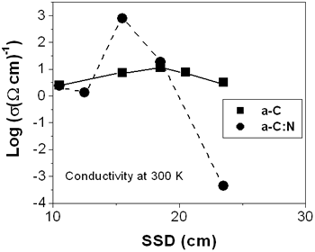
Figure 3. Logarithm of dark electrical conductivity σ versus SSD for samples of a-C and a-C:N. In the case of higher values of σ, a probable doping effect of N is occurring in the material. Figure 4 shows the electron concentration (n), the majority carriers, in the conduction band for a-C and a-C:N films. In the former, n changes from (2.0 ± 0.3)x1020 to (1.1 ± 0.2)x1022 cm-3, however, in the case of a-C:N layers, n varies from (6.5 ± 0.3)x1017 to (4.0 ± 0.2)x1018 cm-3. Taking into account the relationship σ = enμ, where e is electronic charge and μ the mobility, one can deduce that, in general, μ is lower for a-C films than for a-C:N films. 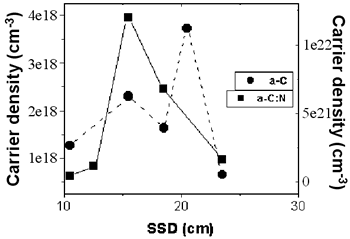
Figure 4. Carrier density versus SSD for a-C and a-C:N samples prepared. Conclusions Physical properties of amorphous carbon films and N-doped amorphous carbon films prepared by the electron gun evaporation technique when the source-substrate distance change in the interval 10.5 – 23.5 cm, were studied. a-C films are constituted of graphitic carbon and identified to be located in the stage I of the FRM with 0% of sp3 sites. a-C:N films were identified to be located in the stage II of the FRM, where a 0 – 20% of sp3 sites can be found. The presence of N in the carbon promotes the presence of these sites. Among all films, the electrical conductivity of the a-C:N sample grown with a SSD of 15.5 cm, was about three orders of magnitude higher than the rest of the samples. However, for films grown with a SSD of 23.5cm the conductivity decreased by nearly seven orders of magnitude. The electrical conductivity of the a-C films remained nearly constant between 1-10 Ω-1cm-1 for all SSD values. Acknowledgements The authors thank Ing. A. B. Soto, M. en C. B. Alvarado-Hidalgo and M. en C. M. Astorga-Cantú by their technical assistance. References 1. A. C. Ferrari and J. Robertson, “Interpretation of Raman spectra of disordered and amorphous carbon“, Phys. Rev., B 61, (2000) 14095. 2. R. Haerle, E. Riedo, A. Pasquarello and A. Baldereschi, “sp2/sp3 hybridization ratio in amorphous carbon from C 1s core-level shifts: X-ray photoelectron spectroscopy and first-principles calculation“, Phys. Rev., B 65, (2001) 045101. 3. A. C. Ferrari, S. E. Rodil, and J. Robertson, “Interpretation of infrared and Raman spectra of amorphous carbon nitrides“, Phys. Rev., B 67, (2003) 155306. Contact Details |