|
RF- magnetron sputtering is widely used to prepare ceramic thin films with more applications in the industry, where the substrate is placed in a low-pressure chamber between two electrodes. The electrodes are driven by an RF power source, which generate a plasma and ionization of argon gas between the electrodes. A DC potential is used to drive the ions towards the surface of the BT-target causing atoms to be knocked off the target and condense on the substrate surface. In the past years, extensive discussion has focused on crystalline phase of nanocrystalline BT, present in powders, bulk bodies or thin films.
Various approaches have been carried out to maximize the remnant polarization in ferroelectrics by using different deposition techniques [3-5]. Enhanced ferroelectricity has been already observed through the use of conducting oxide electrodes [6]. However, oxide electrodes still involve problems such as difficult fabrication, high cost and complicated etching processes and numerous unsolved technical issues remain. High purity indium tin oxide (ITO) (In2O3/SnO2), are widely used as electrical contacts in flat displays, solar cells, detectors, since they are highly conductive and optically transparent [7-8]. Irrespective of its transparency, ITO films has been already successfully used as the conductive metal oxide bottom layers in ferroelectric non-volatile memories.
The problem of using commercial BT-targets is that they fracture during the cathodic erosion, causing heterogeneities in subsequent film deposition procedures. This target degradation can be due to the etching conditions related to the etching zones appearing on targets during the magnetron sputtering process [7], which are determined by the vacuum parameters and also due to the residual stress conditions of the target after sintering at temperatures just below the eutectic temperature (1322°C) between BaTiO3 and the typical TiO2 excess in BT commercial powders.
In the present study, we prepared BaTiO3-thin films by RF-sputtering using low temperature sintered BT-targets from powders processed by high energy ball milling on ITO/Si(111) substrates where ITO thin film is as an electrode. Furthermore, structure and microstructural characterization of the nanocrystalline BT thin films are reported.
Experimental
Targets of BaTiO3 (BT) (50 mm diameter) were prepared starting from BT-commercial powders (99.9%) and particle size of 2 µm, previously dry milled by high energy process (SPEX 8000 mixer mill). The maximal milling time was 120 min, measuring particle size in intervals of 10 min. The evolution of the particle size of the milled powders was monitored by XRD (Rigaku D/Max-2100, radiation CuKa). Powders were uniaxialy pressed at 138 MPa and then sintered at 950°C for one hour in a Felisa-furnace to get several targets with differences in the microstructure.
The ITO/Si(111) substrates consisted on Si(111) wafers with native oxide coated with ITO (1 and 2 min of deposition time). ITO coating was obtained by DC-Magnetron co-sputtering using Sn and In targets. The preparation characteristics of the ITO layer are summarized in the Table 1. Sputtered In and Sn atoms on the Si(111) substrates were post-annealed to form ITO at 550°C/3h in air atmosphere and post-heated at 450°C/1h in a quartz tube furnace (THERMOLYNE-Barnstead-21100) in a N2-H2 atmosphere to improve its conductivity. ITO/Si(111) substrates were characterized by XRD, SEM, AFM, micro-Raman spectroscopy and PFM; In order to exclude the signal of SiO2 in the Raman spectra, Si(111) oxide wafers coated with Ti-Al oxide were previously characterized.
Table 1. Parameters of preparation of the ITO-coated electrodes on Si-substrates.
|
|
|
Work pressure
|
9.1x 10⁻² mBarr
|
|
Ar flux
|
25-30 sccm
|
|
O2 flux
|
5 sccm
|
|
Deposition time
|
1,2,5,6 min
|
|
Substrates
|
Si(111) oxidized
|
The thin films of BT on ITO/Si(111) substrates were obtained by RF-magnetron sputtering (Intercovarmex) using the prepared target that showed the smallest grain size and homogeneous microstructure. The work pressure employed was 10 mTorr with argon and oxygen fluxes of 9.9 sccm and 0.66 sccm, respectively and a power of 75W. Deposition time was varied (90, 150 and 210 min). Thin films of BT were annealed at 600, 700 and 800°C in an oxygen atmosphere using heating and cooling rates procedures of 10º/min. The structure of the thin films of BT was characterized by XRD. The effect of the sintering temperature and deposition time on the process of grain size growth, were monitored and analyzed by XRD and image analysis of AFM micrographs was used to determine secondary growth effects of the films microstructure. Additionally, roughness measurement by AFM was used as criteria to determine the quality of the films. An analysis effect of the growth conditions on the piezoresponse (domains configuration) of the BT films were realized by piezoelectric force microscope (PFM). This system was previously calibrated with a BT oriented (001) crystallite and embedded in a polycrystalline ceramic.
Results and Discussion
BT high energy milled powders reached submicrometric size (360 nm) even after 30 min of milling and less than 280 nm at times up to 120 min. As mentioned before, starting with the powders obtained at 120 min, targets were uniaxially pressed in the desired geometry and after the sintering procedures showed average crystallite and grain sizes of 34 and 360 nm, respectively. The targets presented density values of 86% of the theoretical density and survived the etching conditions during the magnetron sputtering process after preparation of several BT films. The thickness of the prepared BT films prepared with deposition times of 90, 120 and 210 min were 250, 470 and 830 nm, respectively. Crystallite size of the different films was evaluated from XRD being in the range of 16 to 22 nm.
In Figure 1 AFM topography images of the BT-films annealed at 600, 700 and 800°C, where the microstructure can be observed are shown. Figure 1 (a) and (b) show a characteristic equiaxial grain morphology and close to the monodispersion grain size of the films of BaTiO3 obtained at 600 and 700ºC, respectively.
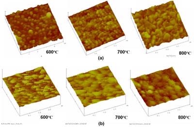
Figure 1. AFM micrographs of the “as coated” BT thin films sintered at 600, 700 and 800°C of a)BaTiO3/ITO-2min/Si(111) and b) BaTiO3/ITO-1min/Si (111).
As the sintering temperature increases a grain growth behavior can be observed. This can best seen in the graphic of Figure 2, where the dependence of the deposition time (90 to 210 min) and sintering temperature on the grain size are shown. Grain size increases e.g. in sample as coated by 150 min from 120 nm to 210 nm when the sintering temperature is increased from 600 to 800ºC, respectively.
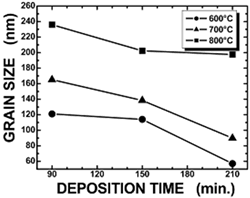
Figure 2. Deposition time dependence on the grain size of BT thin films annealed at 600, 700 and 800ºC.
Microstructure changes in the grain morphology from equiaxial to sharp formed grains as well as strong changes in the surface flatness, measured with the roughness can also be observed by sintering temperatures of 800ºC. The images of Figure 1(b) show surfaces with a very disordered distribution of grains. Formation of agglomerates with nanometric grains can be appreciated clearly as well as higher porosity, resulting in a higher roughness values and fracture of the films. In the left image abnormal grain growth is observed, where non symmetrical big grains embedded in a fine grained matrix are present.
The effects of sintering temperature and deposition time on the grain size are shown in Figure 2. The average grain size of 240 nm was obtained after 90 min of deposition time and sintering at 800°C. With longer deposition times the increment in the grain size was less marked leading to average grain size of 200 nm, as can be seen in Figure 2. This indicates that for longer deposition time (210 min) and sintering temperatures of 800°C, a recrystallization process takes place and not properly a grain growth.
Figure 3 shows the effect in the roughness of BT thin film when the temperature was increased from 600 to 800ºC for different deposition time (90 to 210 min). An increase in the roughness with temperature and deposition time was observed in the films. This result can be related with the increase in grain size with temperature and decrease with deposition time observed in Figure 2.
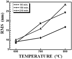
Figure 3. RMS variations as a function of temperature for different deposition times of BT thin films.
Figure 4 shows XRD measurements for the BT thin films growth under the described parameters and annealed at different temperatures. XRD patterns of the prepared films are not very sharp compared with the expected from powders, especially in the films annealed at 600ºC. We can conclude that the chosen sintering range of 600-800°C leads to a crystallization of the BT-films being 600°C the minimal temperature for this purpose.
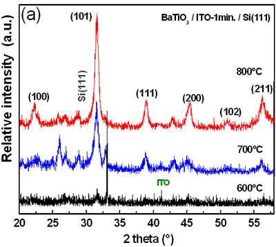
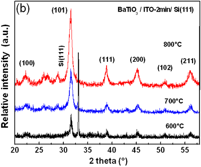
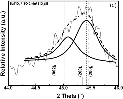
Figure 4. XRD patterns of BaTiO3/ITO-1min/Si(111) thin films heat treated at 600, 700 and 800°C (a,b). A typical deconvolution results for BaTiO3/ITO-2min/Si(111) in the range of 44-46° of 2θ shows the overlapping of the (002) and (200) peaks of the BT tetragonal phase (c).
The main peak of the substrate Si(111) but could be identified, while the absence of ITO peaks can be due to the fact that the layer of ITO is very thin (~10 nm). To get the structure of the films from the XRD results, and as a first approximation it seems that all patterns fit well with the peak positions of standard cubic-phase BT and particularly, the single peak at 2θ = 44.95° is close to the expected value of the (200) plane of BT cubic-phase. The Miller indexes shown in the figure above the peak positions of standard cubic phase were obtained using the BT card JADE#75-2122. Several reports in the literature conclude that the cubic phase in the film can be unmistakably distinguished from tetragonal BT phase since there are two overlapping peaks at 44.85 and 45.38 for tetragonal BT [12-13]. Again, the characteristic splitting of the (200) and (002) in the range 44-46° of 2 θ for the tetragonal BaTiO3 is not clearly observed in the XRD patterns of the prepared BT-films [11]. To get more insight about the structure behavior of BT thin films, a peak deconvolution of the XRD patterns in the mentioned range was undertaken (Figure 4c). The results are shown in Figure 4. From these results, it is clear that the films have a tetragonal phase but under internal stress, so that the lattice parameters are slightly distorted under compressive stress, leading to a broad single peak in the XRD spectra. Further information about this, was obtained by micro-Raman scattering experiments on these films deposited on Ti-Al/Si (111) oxidized substrates (Figure 5). The tetragonal to cubic transition of BT ceramics takes place at about 120°C and in the tetragonal phase, three A1 + E modes arise from three zone-center infrared-active phonons F1u and one, so-called “silent mode”, E + B1 comes from F2u. These modes further split into longitudinal (LO) and transverse (TO) modes due to the long range of electrostatic forces associated with lattice ionicity [13-14]. The appearance of a peak at 305 cm-1 indicates asymmetry within the TiO6 octahedra of BT thin films [15-16]. Therefore, it can be assumed that the formed BT film does not have cubic symmetry. The appearance of the peak at 520 cm-1, corresponding to A1(TO3) mode not can be observed, because the appearance of Si(111) peak at the same wave number.
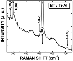
Figure 5. Raman-spectra of BaTiO3/ITO-2min/Si(111) thin films.
The problem of identifying the structure from XRD and micro-Raman measurements is not a new and also not a solved issue. There are several aspects to take into account. First, the critical size below which the abnormal cubic phase is stable at room temperature has been reported in several papers to be, from less than 40 nm [17] to about 190 nm [18].
There is a clear discrepancy of the critical size determination results from different synthesis methods, conditions, and experimental techniques. In the present case, the crystallite size of the prepared films determined by Fourier analysis is around 20 nm. This specific question whether in powders the nanocrystal has a true cubic phase without any tetragonality when it appears to be cubic according XRD results, is an actual discussion theme. For instance, Clark et al. [19] concluded that in powders the nanocrystalline BT particles are tetragonal rather than cubic according to the presence of Raman active modes for the tetragonal phase. In this work we confirmed these conclusions based on the similar measurements and XRD peak deconvolution for the case of BT thin films.
Conclusions
BT-films were successfully fabricated on ITO/Si (111) substrates by RF-sputtering and starting from BT-targets prepared by high energy milling and low temperature sintering. At low sintering temperatures (950°C) best microstructural properties of the target such as: submicrometric grain size (~260 nm), high densification and homogeneity can be obtained. A strong dependence of the annealing temperature on the BT-film microstructure and on the internal stress leading to a distortion of the tetragonal cell was observed. Particularly, at temperatures of 800°C and the longer tested deposition times (210 min) a process of secondary recrystallization was identified. The existence of ferroelectric state through the tetragonal phase in films with grain sizes of 60 nm was verified by micro-Raman, where the presence of A1(TO2) mode, which indicates asymmetry within the TiO6 octahedral was observed. XRD results showed a tetragonal distorted phase manifested as a broad single peak. This detail is the typical evidence of the problem of identifying the structure from XRD and micro-Raman measurements, which is not a new and also not a solved issue. Further work is currently carried out on the characterization of the films by PFM (piezoresponse microscopy).
Acknowledgements
The authors acknowledge technical support from Pedro García Jiménez. Torres-Heredia Victor acknowledges the scholarship assigned by CONACyT during his M. C. program. This work was supported by CONACyT-México.
References
1. C. Feldman, “Formation of thin films of BaTiO3 by evaporation”, Rev. Sci. Instr., 26 [5] (1955) 463.
2. J. Ravez, “Ferroelectricity in solid state chemistry”, Chemistry, 3 (2000) 267-283.
3. R. Thomas, S. Mochizuki, T. Mihara and T. Ishida, “PZT(65/35) and PLZT (8/65/35) thin films by sol-gel process: a comparative study on the structural, microstructural and electrical properties”, thin solid films, 443 (2003) 14-22.
4. M. Foeth, “Determination of the Thermal Broadening of Ferroelectric Domain Walls using Quantitative Transmission Electron Microscopy”, École Polithecnique Fédérale de Laussanne, Switzerland, thesis No 2022 (1999).
5. J. F. Scott, L. Kammerdiner, M. Paris, S. Traynor, V. Ottenbacher, A. Shawabkeh and W. F. Oliver, “Switching kinetics of lead zirconate titanate submicrom thin-film memories”, J. Appl. Phys., 64 [2] (1988) 787-792.
6. T. Sato, T. Kuroiwa, K. Sugahara and H. Ishiwara, “Preparation of Bi3.25+xLa0.75Ti3O12+y films on Ruthenium electrodes”, Jpn. J. Appl. Phys., 41 (2002) 2105-2109.
7. N. W. Jang, S. B. Mah, D. S. Paik, H. W. Choi and C. Y. Park, “Structural and Electrical properties of PLZT films on ITO-coated glass prepared by a sol-gel process”, Materials Research Bulletin, 34, [9] (1999) 1463-1472.
8. J. Pak, K. Nam, J. Lee and G. Park, “Fabrications and electrical properties of ferroelectric Bi3.25La0.75Ti3O12 thin films using a Indium-thin oxide conductive layer as the bottom electrode”, J. Phys.: Condens. Matter., 16 (2004) 4983-4990.
9. G. Golan and A. Axelevitch, “Ring etching zones on magnetron sputtering targets”, Thin Solid Films, 300 (1997) 72-77.
10. Muñoz-Saldaña, B. Mullier and G. A. Schneider, “Preparation of BaTiO3 single crystals using the modified SiO2-exaggerated grain growth method”, J. Eur. Ceram. Soc., 22 (2002) 681-688.
11. M. Hammer, C. Monty, A. Endriss and M. J. Hoffmann, “Correlation between surface texture and chemical composition in undoped, hard, and soft piezoelectric PZT ceramics“, J. Am. Ceram. Soc., 81 [3] (1998) 721-724.
12. M. Wu, R. Xu, S.H. Feng, L. Li, D. Chen and Y.J. Luo, “The influence of anions on the products of BaTiO3 under hydrothermal conditions“, J. Mater. Sci., 31 [23] (1996) 6201-6205.
13. C.T. Xia, E.W. Shi, W.E. Zhong and J.K. Guo, “Preparation of BaTiO3 by the hydrothermal method”, J. Eur. Ceram. Soc., 15 (1995) 1171–1176.
14. A. Dixit, S. B. Majumder, A. Savvinov, R. S. Katiyar, R. Guo and A. S. Bhalla, “Investigations on the sol-gel derived barium zirconium titanate thin films”, Materials Letters, 56 (2002) 933-940.
15. B. Wang and L. Zhang, “Size effects on structure and Raman spectra of BaTiO3 thin films”, Phys. Stat. Sol. (a), 169 (1998) 57-62.
16. J. H. Lee, F. M. Pontes, E. R. Leite, E. Longo, R. Magnani, P. S. Pisan and J. A. Varela, “Effects of post-annealing on the dielectric properties of Au/BaTiO3/Pt thin film capacitors”, Materials Letters, 58 (2004) 1715-1721.
17. H. I. Hsiang and F. S. Yen, “Effect of crystallite size on the ferroelectric domain growth of ultrafine BaTiO3 powders”, J. Am. Ceram. Soc., 79 [4] (1996) 1053–1060.
18. B. D. Begg, E. R. Vance and J. Nowotny, “Effect of particle-sixe on the room-temperature crystal-structure of Barium-Titanate“, J. Am. Ceram. Soc., 77 (1994) 3186.
19. I. J. Clark, T. Takeuchi, N. Ohtori and D. C. Sinclair, “Hydrothermal synthesis and characterisation of BaTiO3 fine powders: precursors, polymorphism and properties”, J. Mater. Chem., 9 (1999) 83-91.
Contact Details
|