Sponsored by VeecoMar 12 2006
Scanning probe microscopes (SPMs) are instruments that measure properties of surfaces. They include atomic force microscopes (AFMs) and scanning tunnelling microscopes (STMs). In their first applications, SPMs were used mainly for measuring 3D surface topography and, although they can now be used to measure many other surface properties, that is still their primary application. SPMs are the most powerful tools of our time for surface metrology, measuring surface features whose dimensions range from interatomic spacing to a tenth of a millimeter.
The main feature that all SPMs have in common is that the measurements are performed with a sharp probe operating in the near field, that is, scanning over the surface while maintaining a very close spacing to the surface. These instruments, specifically STMs, were the first to produce real-space images of atomic arrangements on flat surfaces. SPMs are now most commonly used to perform very precise, three-dimensional measurements on the Ångstrom-to-micrometer scale.
Table 1. Comparison and the characteristics of common microscopes.
|
|
|
Sample Operating Environment
|
Ambient air, liquid or vacuum
|
Vacuum*
|
Ambient air, liquid or vacuum
|
|
Depth of Field
|
Small
|
Large
|
Medium
|
|
Depth of Focus
|
Medium
|
Large
|
Small
|
|
Resolution: X, Y
|
1.0μm
|
5nm
|
2-10nm for AFM
0.1nm for STM
|
|
Resolution: Z
|
n/a
|
n/a
|
0.05nm
|
|
Effective magnification
|
1X – 2x10³X
|
10X – 106X
|
5x10²X – 108X
|
|
Sample preparation requirement
|
Little
|
Little to substantial
|
Little or none
|
|
Characteristics required for sample
|
Sample must not be completely transparent to light wavelength used
|
Surface must not build up charge and must be vacuum compatible
|
Sample must not have local variations in surface height >10 μm
|
XXXXXXXXXXXXXXXXXXXXXX*Environmental SEMs operate at higher pressure and low eV, but resolution is sacrificed.
Until the 1980s, researchers had relied upon other instruments for imaging and measuring the morphology of surfaces. Now in existence for over two decades, SPMs are the newest entry into the surface metrology field. As opposed to optical microscopes and electron microscopes (SEMs, TEMs), SPMs measure surfaces in all three dimensions: X, Y, and Z. Like SEMs, SPMs image and measure the surface of the sample. X and Y topographic resolution for most SPMs, including AFM, is typically 2 to 10 nanometers (STM resolution can be as good as 0.1nm). Z resolution is about 0.1nm for a well-designed AFM or STM.
Optical microscopes and SPMs are the easiest to use, with little or no sample preparation and no vacuum required. Optical microscopes and SEMs can have larger fields of view, but SPMs provide the highest magnifications and resolution in 3D. Furthermore only SPMs work on most samples with minimal sample preparation.
Brief History
The scanning tunneling microscope (STM) was the first SPM technology and was recognized as having atomic resolution capability in 1981.
STM, in fact, still provides the best resolution available (Figure 1). The STM uses the tunneling current between tip and sample to image the sample surface. Unfortunately, there are some limitations, the most significant of which is that the surface of the sample must be conductors or semiconductors. This limits the materials that can be studied.
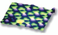
Figure 1. STM image showing single-atom defect in iodine adsorbate lattice on platinum. 2.5nm scan.
This limitation led to the invention in 1986 of the first atomic force microscope. The first commercially available AFM, the Digital Instruments NanoScope® was introduced in 1989. Like the STM, the AFM also uses a very sharp tip to probe and map the morphology of a surface. However, in AFM there is no requirement to measure a current between tip and sample. In this case, the tip is at the end of a micro-fabricated cantilever with a low spring constant. In contact mode AFM, the first AFM technique, the tip-sample force is held fixed by maintaining a constant and very low deflection of the cantilever, pushing the tip against the sample. This force can be in the range of interatomic forces in solids.
Next, we describe the basics of AFM, including how the vertical motion of the tip is detected and transformed into topographic data.
Basic AFM Components
The basic AFM is relatively simple in concept (Figure 2a). Its closest predecessor is the stylus profiler.
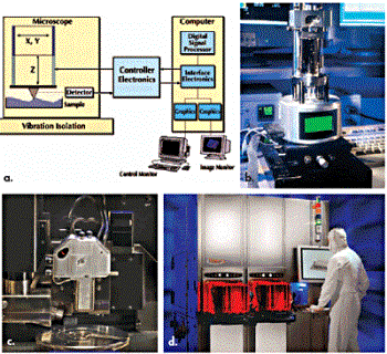
Figure 2. (a) Simplified diagram of a generic AFM. Photos show examples of (b) MultiMode SPM, (c) Dimension 3100 SPM, and (d) fully automated robotic Dimension X3D system for semiconductor applications.
AFM technology uses sharper probes and lower forces than stylus profilers to provide higher resolution information without sample damage. A generic AFM comprises the following components:
- Scanning System
- Probe
- Probe Motion Sensor
- Controller Electronics
- Noise Isolation
- Computer
Scanning System
The most fundamental component of the AFM and the heart of the microscope is the scanner. Depending on the individual design, the scanner may scan (move) the sample (Figure 2b, MultiMode™ SPM) if the sample is small enough, or it may scan the probe over a larger sample (Figure 2c, Dimension™ 3100 SPM).
To accomplish the precision required, a piezoelectric tube scanner is typically used in order to provide sub-Ångstrom motion control.
Probe
Another key component in the system is the probe. As mentioned above, the probe can be stationary and the sample can be scanned under it or the probe can be scanned over the sample. With today’s sophisticated technology, tip/cantilever assemblies that make up the probe (Figure 3) can be mass-produced with consistently shaped, very sharp tips. These tips are integrated into the end of cantilevers, which have a wide range of properties designed for a variety of applications.
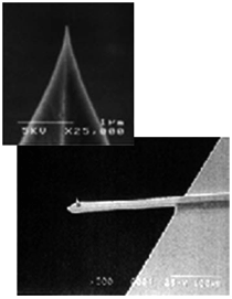
Figure 3. SEM micrograph of an etched single-crystal silicon AFM tip and tip/cantilever assembly
Probe Motion Sensor
This unit senses the force between the probe and the sample and provides a correction signal to the Z portion of the piezoelectric scanner (Figure 2a) to keep the force constant. The most common design for this function is called the optical beam deflection system, which is the lowest noise, most stable, and most versatile system available. This design uses a laser beam shining onto and reflecting off the back of the cantilever and onto a segmented photodiode to measure the probe motion.
Controller Electronics
This unit provides interfacing between the computer, the scanning system and the probe motion sensor. It supplies the voltages that control the piezoelectric scanner, accepts the signal from the probe motion sensor and contains the feedback control electronics for keeping the force between sample and tip constant.
Noise Isolation
To achieve the highest resolution, the microscope must be isolated from noise in its surroundings. There are very effective, yet simple systems for isolating AFM from floor vibrations and from acoustic, electrical and optical noise sources.
Computer
Finally, scanning probe microscopy and AFM would not be feasible without the availability of powerful, high-speed PCs to drive the system and to process, display, and analyse the wealth of data produced.
Applications/Scanning Techniques
In its short lifetime, SPMs has already added many variations to the fundamental scanning tunnelling theme. Once the AFM overcame the severe application limit of STM (the sample conductivity requirement), the variety of techniques and the range of applications began to mushroom. Although topographic mapping is still the dominant application for AFM (Figure 4), commercially available SPMs now provide some or all of the following techniques:
Scanning Tunneling Microscopy
Scanning Tunnelling Microscopy (STM) measures topography using the tunneling current between the probe tip and a conductive sample surface.
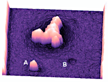
Figure 4. Detailed topography of three defects – two protrusions and a depression – in a phase-shift photolithography mask. A cross section measures the smaller of the two protrusions (A) ~140nm across in the plane of the image. The depression defect (B) measures less than 6nm deep. 1.5μm scan.
Contact Mode AFM
Contact Mode AFM measures topography with the probe perpetually in contact with the sample.
TappingMode AFM
TappingMode AFM (patented) measures topography by lightly tapping the surface with an oscillating probe tip. Eliminates shear forces (present in contact mode). TappingMode is now the scanning mode of choice for most applications, particularly for softer surfaces like polymers.
Non-contact Mode AFM
Non-contact Mode AFM measures topography by sensing Van der Waals attraction between surface and probe tip.
It is less stable than either contact or TappingMode.
LiftMode
LiftMode (patented) is a two-pass technique that separately measures topography and another selected property (magnetic force, electric force, etc.) using topographic information to track the probe tip at a constant distance above the surface.
PhaseImaging
PhaseImaging (patented) maps surface composition based on differences in local mechanical or adhesive properties of the sample.
Lateral Force Microscopy
Lateral Force Microscopy (LFM) maps frictional forces between the probe tip and the sample surface. The tip can be functionalized with chemical species for chemical force microscopy.
Magnetic Force Microscopy
Magnetic Force Microscopy (MFM) maps magnetic force gradient and distribution above the sample surface using LiftMode (Figure 5).
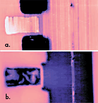
Figure 5. AFM (a) and LiftMode MFM (b) images of pole tip region on magnetoresistive (MR) read/write head used in computer hard drives. MFM image shows domain structure and MR sensor that cannot be seen in the AFM topography. 12μm scan.
Force Modulation
Force Modulation (patented) maps relative stiffness of surface features.
Electric Force Microscopy
Electric Force Microscopy (EFM) maps electric field gradient and distribution above the sample surface using LiftMode.
Surface Potential Imaging
Surface Potential Imaging is one of the few AFM techniques that makes quantifiable maps of a quantity other than surface topography. Using LiftMode, it maps the distribution of surface electric potential of the sample. Recent applications include corrosion studies of alloys.
Electrochemical SPM
Electrochemical SPM maps topographic changes in-situ as induced by electrochemical reactions in electrolyte solutions simultaneously with electrochemical cell potential control (e.g. voltammetry). Can be performed with AFM or STM.
Scanning Electrochemical Potential Microscopy
Scanning Electrochemical Potential Microscopy (SECPM) (patented) is in-situ imaging or potential mapping of the electrode surface by measuring the potential difference between the potentiometric probe and the sample immersed in an electrolyte solution or a polar liquid (Figure 6).
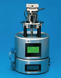
Figure 6. Scanning electrochemical potential microscope (SECPM).
Scanning Capacitance Microscopy and Scanning Spreading Resistance Microscopy
Scanning Capacitance Microscopy (SCM) and Scanning Spreading Resistance Microscopy (SSRM) both map 2D carrier (dopant) concentration profiles in semiconductor materials.
Scanning Thermal Microscopy
Scanning Thermal Microscopy (SThM) maps surface temperature distribution.
Tunneling AFM and Conductive AFM
Tunneling AFM and Conductive AFM measure tip-sample current for characterization of electrical conductivity and evaluation of thin film integrity.
TRmode
TRmode maps lateral forces and force gradients. Interleaves with TappingMode for complementary lateral and vertical characterization (Figure 7).
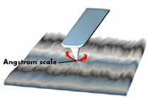
Figure 7. TRmode is a technique that uses torsional oscillations of an AFM probe.
Nanoindenting
Nanoindenting measures mechanical properties and wear characteristics (hardness, adhesion, durability) of thin films, polymers, etc. (e.g. dielectrics, DLC).
These techniques are being applied to a wide array of application areas, from biology to semiconductors, from data storage devices to polymers, and from integrated optics to measurement of forces between particles and surfaces. Other applications include MEMS fabrication, paints and coatings, metals/alloys/platings, plastics/polymers, biomaterials, biotechnology, food and food packaging, optics/optical films, optical disks, ceramics, thin films, liquid crystals, cosmetics, and geological and environmental studies.
In addition, AFM systems have already been developed for highly specific applications, including automated robotic systems for handling semiconductor wafers (Figure 2d). They have also been developed with analysis routines designed for specific applications such as CD and DVD bump/pit measurements, as well as pole tip recession measurements for data storage read/write head manufacturing. These applications continue to expand.
Environmental Controls
AFM applications are carried out in a variety of environments. AFM can be operated in ambient air, in vacuum, and in liquids (Figure 8). Biological measurements, in particular, are often carried out in-vitro in liquids. Electrochemical experiments are performed in liquid cells, allowing atomic-scale observation of electrochemical processes. In some cases, surface cleaning studies are done at atmospheric pressure in the controlled environment of a dry glove box.
Figure 8. Condensed deoxyribonucleic acid (DNA) has been proposed as a gene delivery mechanism for biotechnology applications. Here, unfixed molecules were imaged in salt solution. 20μm scan.
Recent new products include heating systems for biological and polymer applications up to 250°C (Figure 9), complete with sophisticated sample and environmental sensing. Systems are also now available for controlling the gaseous environment of the sample under study (Figures 10a and b).
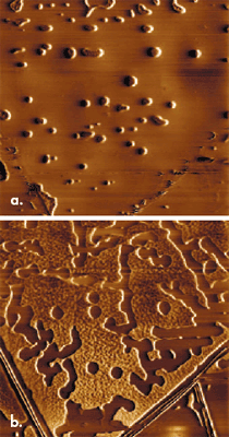
Figure 9. Successive phase images of poly(hexacyclodimethyl)siloxane at (a) 85ºC and (b) 90ºC. Heating induces formation of liquid islands within the amorphous polymers (a), which convert into arrays of small dots on additional heating (b). 10μm scans.
Figure 10a. The Atmospheric Hood for the MultiMode SPM allows control of the gaseous imaging environment to vary humidity or image under inert gases.
Figure 10b. The EnviroScope offers high vacuum, heating, electrochemical cell potential control, and purged gas environment.
Recent Technology Advances
New hardware and software have extended the utility of high-end SPM systems beyond measurement and characterization to include nanomanipulation and nanolithography.
Examples of in-plane and out-of-plane nanomanipulation are shown in Figures 11a and 11b. An example of point-and-click nanolithography is seen in Figure 11c.
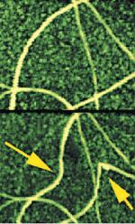
Figure 11a. AFM in-plane nanomanipulation uses the AFM probe to image, manipulate nanometer-scale objects (carbon nanotubes), and image again to see the results.
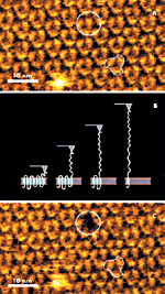
Figure 11b. AFM out-of-plane nanomanipulation uses the AFM probe to image, pull a single biomolecule out of the plane of the sample while measuring the unfolding of the molecule, and image again to see the results (in this case, the removal of one molecule from an array).
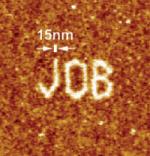
Figure 11c. AFM nanolithography.
New controllers and electronics (e.g., the NanoScope IV and IVa SPM controllers) have been designed to enhance performance relative to traditional designs. Some of the recent developments in AFM technology include:
Combined Environmental Controls
The latest generation of SPMs offer combinations of environmental controls, including vacuum and high temperature (Figure 12).
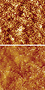
Figure 12. Poly-sbs at room temperature in air (a) and at 180°C in 10-5 Torr pressure (b). Images captured with the Enviroscope (Figure 10b).
Higher lateral resolution
AFM systems now provide higher data density to allow zooming into the finest details, even on large scans. This provides the resolution required to characterize sidewalls on such samples as DVD bumps/pits and semiconductors. It also allows observation and measurement of nanoscale details on large scans — without the need to spend additional time re-scanning the sample with a smaller scan area (Figure 13).
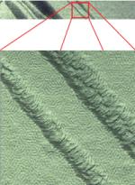
Figure 13. TappingMode+ height image and zoom of a copolymer. The square image is a zoom into the boxed area in the original rectangular image. This detail is revealed by simply zooming in with software and without the need for time-consuming, repetitive smaller scans. Without this higher resolution scanning, the zoomed image would not have the pixel resolution required to view nanoscale details. 10μm x 1.24μm scan and 1μm x 1μm zoom.
“Q”– Control
Controlling the quality factor, or Q, of the oscillating AFM probe allows better control of the forces between tip and sample and improves the sensitivity of measurements such as with PhaseImaging and MFM (Figure 14).
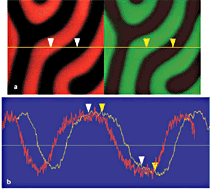
Figure 14. Images of the same area on magnetic recording tape scanned with and without Q-control. Phase detection MFM images and average cross-section measurements of the probe phase shift illustrate nearly 4x enhanced signal-to-noise ratio for the Q-controlled image. 15μm scans.
Summary
Scanning tunneling microscopy produced dramatic images of atomic lattices and atomic force microscopy broadened the technology to non-conductive surfaces. Development of atomic force microscopes has allowed scientists and engineers to see structure and detail with unprecedented resolution and without the need for rigorous sample preparation. Several advances have further extended this technique’s utility to a wide range of applications.
TappingMode permits imaging of soft materials without damage to the sample and LiftMode allows separate but simultaneous imaging of topography and other parameters, such as magnetic or electric forces, without cross-contamination.
PhaseImaging has opened up the capability for mapping of surface compositional variations. New scanning and measurement technologies have expanded the range of measurements and thus further increased the utility of AFM for a broad variety of applications.
These developments have taken AFM, in a few short years, from a laboratory curiosity to one of the most powerful, flexible, and widely used technologies for surface characterization.
.png)
This information has been sourced, reviewed and adapted from materials provided by Veeco.
For more information on this source, please visit Veeco.