Introduction
Deep ultraviolet light emissive materials are very attractive, because it can realize the unexplored advanced-optoelectronics such as ultra high-density optical data storage and flat panel display in next generation. Beta gallium oxide (β-Ga2O3) is very attractive material for deep ultraviolet (DUV) optoelectronics because of its wide band gap approximately 4.8 eV [1]. To utilize β-Ga2O3 as optoelectronic devices, it is necessary to investigate the luminescence properties. Cathodoluminescence is one of the practical techniques to estimate the luminescence properties of wide band gap semiconductors.
Some groups [2-4] reported the luminescence properties of β-Ga2O3 which were synthesized by various methods. However, visible blue/green emissions were dominant over the desirable deep ultraviolet emissions in their reports. The material exhibits n-type conductivity originating from existing oxygen vacancies [5,6] and the visible emissions were attributed to these defects [7-9].
Nezaki et al. [10, 11] discovered a novel crystal growth technique named “electric current heating method”. ZnO crystals grown by this method exhibit the ultraviolet emission corresponding to the band gap of ZnO.
We have recently succeeded in synthesizing blue / ultraviolet emissive β-Ga2O3 crystals by electric current heating method in vacuum [12]. Furthermore, β-Ga2O3 crystal with high monochromatic ultraviolet emission was obtained by optimizing ambient temperature for the crystal growth [13]. Nevertheless, required deep ultraviolet emission was not observed at β-Ga2O3.
In order to elucidate the origin of ultraviolet and visible emission observed at β-Ga2O3, Harwig et al. [14, 15] reported the effect of small amount of several oxides as dopant on the luminescence of β-Ga2O3 powders and single crystals. However, the effect of large amount of doping on the luminescence of β-Ga2O3 was not investigated.
The extensive solid solution was obtained from the solid state reaction of β-Ga2O3 – α-Al2O3 [16]. Therefore, the system of β-Ga2O3 – α-Al2O3 is feasible for investigating the luminescence properties of β-Ga2O3 with a large amount of doping.
In this paper, a deep ultraviolet emissive material synthesized in compositionally graded solid solution between β-Ga2O3 and α-Al2O3 was investigated by a novel method combining with the coupling of ceramics, cathodoluminescence (CL) and energy dispersive X-ray spectroscopy (EDS).
Experimental Procedure
A powder of β-Ga2O3 (Kojundo Chemical Laboratory, 99.99% purity) and α-Al2O3 (Taimei Chemical, 99.99% purity) were pressed into pellets (φ 20 mm x 5 mm) at 200 MPa and sintered at 1700oC for 24 h in air individually. The sintered pellets were polished, contacted each other and heated at 1700oC for 24 h in air. After the heat treatment, the pellets were stuck together. The sample was encapsuled in conductive resin and cut perpendicularly to the interface with a diamond cutter. The cut surface was polished and coated with Au by vacuum spattering in order to avoid charge-up.
The morphology and elemental distribution of the sample surface was observed using a scanning electron microscope (SEM; JEOL, JSM-5510) and EDS (JEOL, JED-2201), respectively. Cathodoluminescence of the sample was measured using electron beam accelerated by 20 kV at room temperature. The luminescence was collected using an ellipsoidal mirror and led into a monochromator (Jobin Yvon, TRIAX-320) through an optical quartz fiber. A grating (150 lines/mm) and CCD detector (Jobin Yvon, CCD1024x256-0) were employed in the monochromator for spectral detection.
Results and Discussion
Figure 1 shows SEM image and EDS elemental maps of Ga and Al for the diffusion interface of the sample. In the elemental maps, the white area indicates a high concentration of the elements. In the SEM image, clear boundary between β-Ga2O3 and α-Al2O3 was not observed. The result of EDS analysis indicated graded distribution of Ga and Al near the interface. These smooth elemental distributions were considered to show the compositionally graded solid solution between β-Ga2O3 and α-Al2O3.
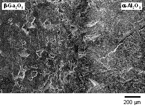
(a) SEM
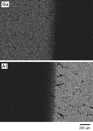
(b) EDS
Figure 1. SEM image (a) and EDS elemental maps (b), observed near the interface of β-Ga2O3 and α-Al2O3.
Figure 2 shows cathodoluminescence spectra observed across the diffusion layer of β-Ga2O3 and α-Al2O3. Each spectrum marked with a to q shown in (A) was observed at white points marked with a~q shown in (B). In the part of β-Ga2O3 (a to c), the spectra showed weak emissions. On the other hand, the spectra observed near the interface (d to i) showed intense emissions with broad distribution from blue to ultraviolet. These spectra corresponded to the results in previous reports [12, 13]. Furthermore, the intensity of the blue emission around 2.9 eV was decreased in the part close to the interface (i), and intense ultraviolet emission peaked at 3.5 eV was clearly observed. In the middle of diffusion layer (j), the observed spectrum showed very weak emission.
The spectra observed near the interface (k~n) showed intense emissions with broad distribution from ultraviolet to deep ultraviolet. Furthermore, these spectra contain novel peaks at 4.1 eV and 4.5 eV. In the part of α-Al2O3 (o~q), the spectra showed weak emissions.
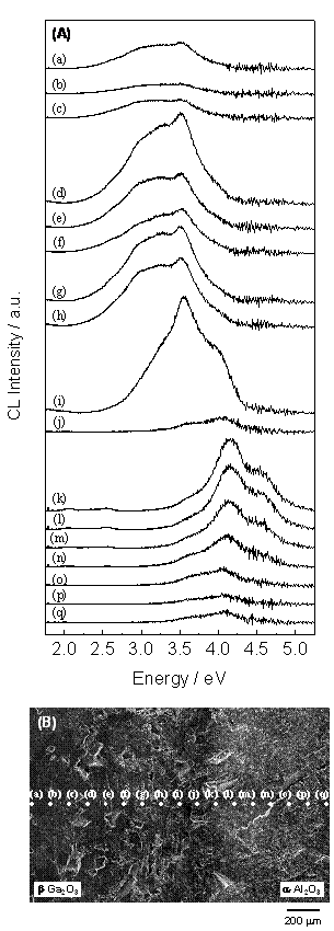
Figure 2. Cathodoluminescence spectra. The spectra (A) were observed at white points shown in (B).
Figure 3 shows the relation between EDS elemental concentration and CL intensity distribution of blue (2.9 eV), ultraviolet (3.5 eV) and deep ultraviolet (4.1 and 4.5 eV) emissions observed across the diffusion interface between β-Ga2O3 and α-Al2O3.
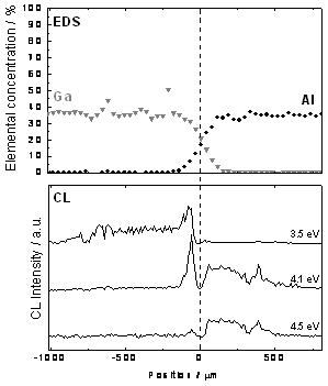
Figure 3. Relation between elemental concentration and cathodoluminescence intensity observed near the boundary between β-Ga2O3 and α-Al2O3.
In the compositionally graded layer, Ga rich area showed both ultraviolet (3.5 eV) and deep ultraviolet (4.1 eV) emissions. On the other hand Al rich area shows deep ultraviolet (4.1 eV and 4.5 eV) emissions. In addition, the area where the amount of Ga and Al was almost the same, showed very weak emission.
The origin of ultraviolet and deep ultraviolet emission observed at Ga rich area is considered to be β-Ga2O3 based solid solution. Furthermore, the origin of deep ultraviolet emission observed at Al rich area is considered to be α-Al2O3 based solid solution. On the other hand, the cause of the weak emission observed at middle of β-Ga2O3 and α-Al2O3 is thought to be GaAlO3, resulting from the binary compound of β-Ga2O3 and α-Al2O3.
Summary
Cathodoluminescence and elemental composition in diffusion layer synthesized by coupling of β-Ga2O3 and α-Al2O3 was investigated. At diffusion interface, Ga rich area showed ultraviolet (3.5 eV) and deep ultraviolet (4.1 eV) emissions, on the other hand, Al rich area showed deep ultraviolet (4.1 and 4.5 eV) emissions. These results suggest that the solid solution of β-Ga2O3 and α-Al2O3 is attractive material for ultraviolet and/or deep ultraviolet optoelectronics. Furthermore, the investigation method combining with the coupling, CL and EDS is very practical for finding novel optoelectronic materials.
Acknowledgements
This study was supported in part by a Grant for 21st Century COE Program "Creation of Hybridized Materials with Super-Functions and Formation of International Research & Education Center" from the Ministry of Education, Culture, Sports, Science, and Technology of Japan.
References
1. H. H. Tippins, “Optical Absorption and Photoconductivity in the Band Edge of β-Ga2O3”, Phys. Rev. A, 140, 316-319 (1965).
2. D. P.Yu, J. -L. Bubendorff, J. F. Zhou, Y. Leprince-Wang and M. Troyon, “Localized cathodoluminescence investigation on single Ga2O3 nanoribbon/nanowire”, Solid State Comm., 124, 417-421 (2002).
3. C. H. Liang, G. W. Meng, G. Z. Wang, Y. W. Wang, L. D. Zhang and S. Y. Zhang, “Catalytic synthesis and photoluminescence of β-Ga2O3 nanowires”, Appl. Phys. Lett., 78, 3202-3204 (2001).
4. E. G. Villora, T. Atou, T. Sekiguchi, T. Sugawara, M. Kikuchi and T. Fukuda, “Cathodoluminescence of undoped β-Ga2O3 single crystals”, Solid State Commun., 120, 455-458 (2001).
5. T. Harwig, G. J. Wubs and G. J. Dirksen, “Electrical properties of β-Ga2O3 single crystals”, Solid State Commun., 18, 1223-1225 (1976).
6. T. Harwig and J. Schoonman, “Electrical Properties of b-Ga2O3 Single Crystals. II”, J. Solid State Chem., 23, 205-211 (1978).
7. T. Harwig, F. Kellendonk and S. Slappendel, “The ultraviolet luminescence of β-galliumsesquioxide”, J. Phys. Chem. Solids, 39, 675-680 (1978).
8. L. BINET and D. GOURIER, “Origin of the blue luminescence of β-Ga2O3”, J. Phys. Chem. Solids, 59 (1998) 1241-1249.
9. E. G. Villora, M. Yamaga, T. Inoue, S. Yabasi, Y. Masui, T. Sugawara and T. Fukuda, “Optical Spectroscopy Study on β-Ga2O3”, Jpn. J. Appl. Phys., 41, 622-625 (2002).
10. D. Nezaki, S. Takano, Y. Kuroki, Y. Kurihara, T. Okamoto and M. Takata, “Crystal Growth on ZnO Ceramics Heated by Direct Current”, Trans. Mater. Res. Soc. Jpn., 25, 205-208 (2000).
11. D. Nezaki, T. Okamoto and M. Takata, “Structure and Photoluminescence of ZnO Crystals Grown by Electric Current Heating Method”, Key Eng. Mater., 228-229, 241-244 (2002).
12. K. Suzuki, T. Okamoto and M. Takata, “Crystal growth of β-Ga2O3 by electric current heating method”, Ceramics International, 30, 1679-1683 (2004).
13. K. Suzuki, Y. Kuroki, T. Okamoto and M. Takata, “Effect of Growth Conditions on the Cathodoluminescence of β-Ga2O3 Crystals Grown by Electric Current Heating Method”, Key Eng. Mater., 301, 181-184 (2006)
14. T. Harwig and F. Kellendonk, “Some Observations on the Photoluminescence of Doped β-Galliumsesquioxide”, J. Solid State Chem. 24, 255-263 (1978).
15. T. Harwig, F. Kellendonk and S. Slappendel, “The ultraviolet luminescence of β-galliumsesquioxide”, J. Phys. Chem. Solids 39, 675-680 (1978).
16. V. G. Hill, R. Roy and E. F. Oaborn, “The system Alumina – Gallia - Water”, J. Am. Ceram. Soc., 35 [6], 135-142 (1952).
Contact Details
|