It is essential that high aspect ratios are maintained in thick film and screen printing technology. One must ensure that thick film paste maintains good printability throughout the time on the screen and the screen parameters allow for high throughput and repeatability of results. This article discusses the interactions of thick film paste and screen printing technology in the effort to achieve high aspect ratio and fine line patterns.
Thick Film Technology
Thick film paste is a suspension of a functional conductive phase, vehicle, binder and additives for solar metallization applications. Silver is the most common conductive filler used for front contact paste. The binder comprises a glass frit that is used to bind the functional phase to the silicon wafer. Critical choices in materials must be made to determine the ideal balance of properties for screen printable pastes suitable for high aspect ratios. The paste must transfer through the mesh material of the screen and the emulsion coating and adhere to the wafer. The wafer surfaces are textured to increase the probability of light absorption, and this provides additional difficulty for the screen printing process.
Screen Technology
Screen technology plays a very essential role in paste transfer. Most solar cell manufacturers use basic screen printing techniques. Paste is removed through a patterned screen for deposition on a silicon wafer using a squeegee. Fine mesh screens enable intricate patterns of solar cell grid designs.
Stainless steel mesh is used by most solar cell manufacturers for the front side metallization process. However, finer diameter wires also lead to lower theoretical line heights which are detrimental to high aspect ratio. The emulsion is a UV imageable material that has been customized for solvent resistance, durability, and exposure characteristics. A screen is exposed for a specific amount of time under a UV lamp during the patterning process. Imaging time increases with the mesh count (number of wires per inch or cm) and emulsion thickness. A photopositive is placed in front of the emulsion to block the light from hardening that area. After exposure, the emulsion of the un-reacted area is washed out.
Experimental Method
For this study, Sefar Printing Solutions offered a range of stainless steel meshes and emulsion thicknesses that were used to examine the impact on fine line resolution and aspect ratio. An industry standard paste, Heraeus SOL950, was used for initial testing.
A range of finger line widths from 60µm to 100µm in increments of 10µm were designed in a pattern that was printed on one c-Si wafer. The different parameters calculated are:
- Aspect Ratio: Aspect Ratio was calculated by the following formula - Height (µm)/Width (µm)
- Line Width: Line width was measured in microns using a calibrated PaxCam3 digital camera system with PaxIt software.
- Line Height: Line height was measured in microns using a Cyber Vantage Laser Profilometer 3-D measurement system. A 1cm area on one line from each group of widths was scanned. The average line height was recorded.
- Line resistance: Line resistance was measured using a 4-point probe system from GP Solar. The wafers were cut with a dicing saw into 7cm widths, and each line resistance was measured. Units for line resistance are Ohm/cm.
Table 1. Screen meshes and emulsion thicknesses with the appropriate open area percentages
| Mesh Count (wires/in.) |
Wire Diameter (μm) |
Open Area (%) |
EOM (μm) |
| 280 |
25 |
52.5 |
8, 15, 24 |
| 290 |
20 |
59.5 |
9, 19, 24 |
| 360 |
16 |
59.8 |
10, 19, 27 |
| 500 |
18 |
41.7 |
8, 18, 23 |
Table 2. Printing parameters
| Frame Size |
12"x12" |
| Off-Contact |
1.2mm |
| Pressure |
96N |
| Print Speed |
200mm/sec |
| Squeegee Durometer |
80A |
Results and Discussion
Percent open area of the particular screen meshes had the largest impact on aspect ratio and line resistance as shown in Figure 1. Line resistance decreased with increasing open area, and the aspect ratio increased.
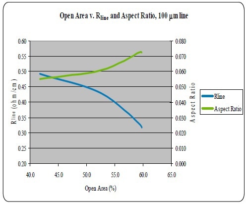
Figure 1. Open Area % v. Rline and Aspect Ratio. Averaged data from the 100µm finger line openings
A visual comparison of open area can be seen in Figures 2 and 3 for the 280 mesh and 360 mesh, respectively. Furthermore, the area that the larger wire of the 280 mesh occupies near the edges of the finger line makes paste transfer challenging. Both of these screen meshes are used in solar cell manufacturing, but there are cost differences between them.
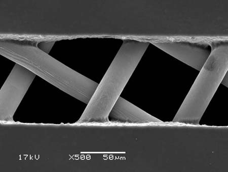
Figure 2. 280 mesh, 25µm wire diameter, 100µm finger line opening, 24µm EOM. Open area is 52.5%. SEM photo is directly over finger line opening, 500x
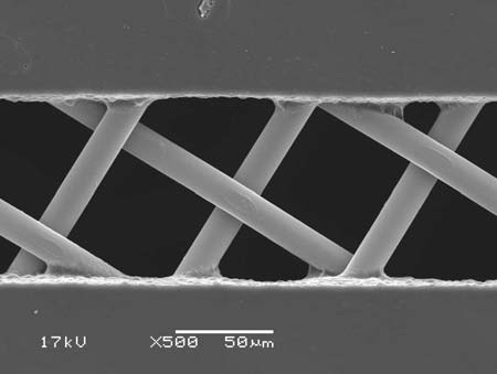
Figure 3. 360 mesh screen, 15µm wire diameter, 100µm finger line opening, 27µm EOM. Open area is 60.0%. SEM photo is directly over finger line opening, 500x
Table 3 provides interesting data to support the influence of open area. Though the theoretical print thickness for the 280 mesh, 24µm EOM is approximately 10% higher than the 360 mesh, 27µm EOM, the actual fired film thickness is 17% lower.
Table 3. Comparison of data for 280 mesh and 360 mesh for the highest emulsion thickness
| 100μm Finger line |
280, 24μm EOM |
360, 27μm EOM |
| Width |
104.9 |
107.6 |
| Height |
6.5 |
7.8 |
| Aspect Ratio |
0.062 |
0.073 |
| Rline |
0.43 |
0.34 |
Theoretical thickness is calculated by:
[(2 x wire diameter) x open area %] + EOM
Despite the thicker EOM, the larger open area of the 360 mesh was more influential on paste transfer.
Figure 4 shows the influence of emulsion thickness on line height and aspect ratio. The data did not show a dramatic increase in line height or improvement in aspect ratio by increasing the EOM thickness.
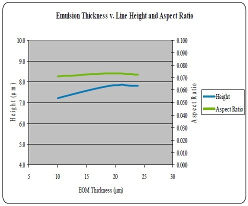
Figure 4. Emulsion Thickness v. Line Height and Aspect Ratio. 360 mesh screen, 15µm wire diameter
Figures 5 and 6 provide a good view of the emulsion side walls. As evident, the walls are not perfectly smooth, and the paste will adhere to that surface when it passes through the screen.
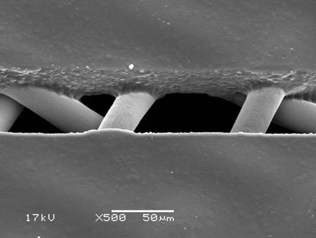
Figure 5. 280 mesh, 25µm wire diameter, 60µm finger line opening, 24µm EOM. SEM photo was taken at 30° from the top view, 500x
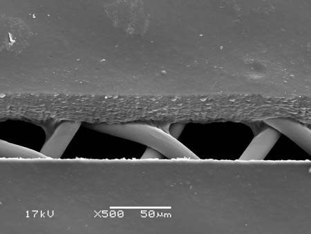
Figure 6. 360 mesh, 15µm wire diameter, 60µm finger line opening, 27µm EOM. SEM photo was taken at 30° from the top view, 500x
Conclusion
Crystalline silicon solar cell manufacturing is advancing toward higher sheet resistance emitters to improve conversion efficiencies. The front grid design must be modified to have narrower lines with finer pitch to account for the increased resistance and minimize shading of the cell. Thick film paste formulations and screen technology faces the challenge of providing these materials with fine line printing capabilities while providing sufficient current transport. Additional line height is required to accomplish this low line resistance, so the aspect ratio of the paste formulation is critical.
About Heraeus Photovoltaics
The Heraeus Photovoltaics Business Unit is an industry leading developer and manufacturer of metallization pastes for the photovoltaic industry.
Heraeus has been a manufacturer of thick film pastes for over 40 years. Since 2008, we have been an innovative supplier to the photovoltaics industry, working with c-Si cell manufacturers to improve their cells’ efficiency for both conventional and advanced cell designs.
Heraeus have developed silver metallization pastes that have been integrated into commercially available technologies such as MWT, Double Print, Dual Printing, Selective Emitter, Back Side Passivation and N-Type Cells.
Heraeus have also expanded our capabilities and developed lower temperature processing pastes for Thin Film and other c-Si technologies.
Heraeus' goal is to improve our customers’ cell efficiency and reduce their cell’s cost per watt through our innovative paste design technology.

This information has been sourced, reviewed and adapted from materials provided by Heraeus Photovoltaics.
For the original article, please visit Heraeus Photovoltaics white papers and articles.