Sponsored by HORIBAOct 28 2013
Raman spectroscopy is a proven technology in the analysis of the basic properties of semiconductors, especially in ascertaining the characteristics of microelectronic devices for the reason that the performance of SiGe-based devices greatly rely on the knowledge of the Ge content, composition and the strain of the layers. In addition, measuring strain and alloy composition in semiconductor structures is imperative for calibrating growth processes and controlling the electrical and optical characteristics of these materials.
For probing mechanical stress using Raman spectroscopy, the material to be analyzed needs to show Raman active modes in the spectrum. Mechanical strain can elevate the degeneracy of Raman modes by affecting their frequency positions. Hence, the strain can be observed and detected by monitoring the shift in the band position. Moreover, the band shape can also be affected by the strain, inducing broadening and deformation of peaks. These effects rely upon the strain geometry and material characteristics. The characteristic structure of the sample (Sample 1) analyzed is illustrated in Figure 1. This article highlights the selection of the laser excitation and measurement conditions and discusses the results acquired in the visible and in the UV range.
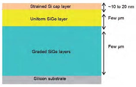
Figure 1. Typical structure of Si/SiGe/Si sample
Influence of the Laser
The selection of the laser excitation will have an influence on various parameters:
- The fluorescence level that may corrupt Raman signal
- The probing volume that relies on the beam penetration and laser spot size
- The signal acquisition, for the reason that the Raman intensity is directly proportional to (1/λ)
- The resonance effect where some Raman bands show strong wavelength dependence
- The coverage and resolution because of the variation of the grating dispersion along the spectral range
For strongly absorbing materials like most semiconductors, the Raman signal derives from a volume defined by the diameter and penetration depth of the laser beam. A shorter laser wavelength causes lower penetration, thereby providing details on the strain closer to the surface. Different excitation wavelengths and respective penetration depths in silicon and germanium are listed in Table 1.
Table 1. Penetration depths in Si and Ge influence of the excitation wavelength
| Laser wavelength (nm) |
Penetration depth in Si (nm) |
Penetration depth in Ge (nm) |
| 633 |
3000 |
32 |
| 514 |
762 |
19.2 |
| 488 |
569 |
19 |
| 457 |
313 |
18.7 |
| 325 |
∼10 |
∼9 |
| 244 |
∼6 |
∼7 |
The spatial discrimination is limited by the generally applied visible excitations in both axial and lateral dimensions. UV micro Raman can optimize the spatial resolution by leveraging the much smaller optical penetration depth and shorter wavelength. Additionally, the much shorter optical penetration depth in the UV (~10nm at 325nm in Si) enables the analysis of shallow active layers.
The influence of the laser selection is demonstrated in Figure 3, illustrating the spectra acquired at various wavelengths on the sample depicted in Figure 1. The combination of visible and UV measurements is useful for samples with a structure as shown in Figure 1.
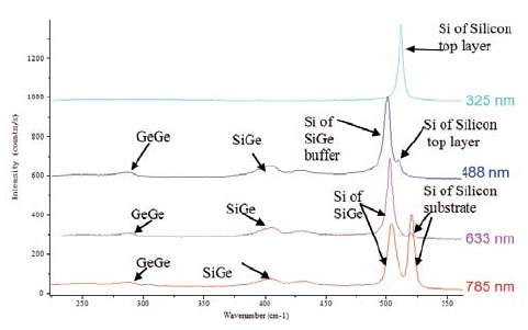
Figure 2. Spectra recorded at 325, 488, 633 and 785nm on sample 1
Measurement Conditions
In terms of experimental definition and instrumental configuration, many different parameters have to be taken into account to improve the accuracy and consistency of the information. To begin with, the use of a reference band can improve the determination of the peak position. This will also enable eliminating the effect of external parameters like environmental temperature, which can influence the frequency of the Raman peak being monitored.
This reference needs to be acquired concurrently with the Raman band. For this reason, the plasma lines from the laser source itself are more suitable as they deliver sharp emission of well known frequency, which are collinear with the Raman spectra. These spectra will be subsequently corrected corresponding to the plasma position. Furthermore, the use of an autofocus device is also essential as it enables maintaining proper illumination, ensuring the plasma position, correcting for any sample tilt or surface roughness.
The localized heating of the sample is also of importance as it can affect the strain measurement. If the laser power density is very high, the sample can be heated at the point of focus, causing a temperature induced down-shift of the Raman peak. Hence, low laser powers, typically at a sub mW level, are generally recommended.
Results
Visible Raman spectrum
The 488nm line of an Argon laser was used in the sample characterization. At 488nm, the Raman signal coming from the SiGe layer dominates the spectrum owing to the aforementioned penetration effect (Figure 4). The spectrum analysis reveals the difficulty to acquire precisely the positions of the SiGe and GeGe modes because of the weaker intensity, asymmetric shape, and larger width of these lines. However, the position of the SiGe and GeGe bands can be more precisely acquired with the higher signal to noise ratio.
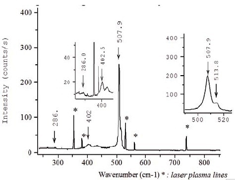
Figure 3. Raman spectrum acquired at 488nm
UV Raman Spectrum
The Raman spectrum of sample 1 acquired at 325nm is depicted in Figure 5. Since the bands of the SiGe layer are dominant in the visible spectrum (Figure 4), accurately identifying the position of the peak of the Silicon cap layer is a difficult task, although the peak is visible but appears as a shoulder. From Table 1, it can be observed that the penetration depths of different laser lines for the silicon material are a few nanometers in the UV range, suggesting the use of UV excitation line in the analysis of thin silicon layers. Consequently, the UV Raman spectrum of sample 1 illustrated in Figure 5 only exhibits the silicon peak of the thin top layer, thereby enabling to define the position of the Silicon line ωSi from this cap layer.
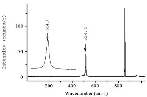
Figure 4. Raman spectrum acquired at 325nm
Correlating Spectroscopic Data with Sample Composition and Strain
The position of the SiSi and SiGe modes of the SiGe layer can be obtained from the visible Raman spectrum. The following formula correlates Ge content (x) to the SiSi phonon peak position ωSiSi for thick layers of relaxed SiGe alloy:
ωSiSi= 520.0-68x
For thinner layers and values of x close to 0.3, the formulae will be:
ωSi = 520.2-62x equation 1
ωSiGe= 400.5+14.2x equation 2
Considering the strain ε, the formulae become:
ωSiSi = 520.2-62x –815e equation 1b
ωSiGe = 400.5+14.2x-575e equation 2b
ωGeGe = 282.5+16x-385e equation 3b
Using these formulae, the Ge content and strain or degree of relaxation can be estimated depending on the Raman spectrum of the film. These formulae are applicable for visible excitation Raman spectra.
Conclusion
The results clearly demonstrate the capability of Raman spectroscopy in the determination of Ge fraction and strain in SiGe layers and Si cap layers, as the technique allows the use of both visible and UV excitation lines on a single instrument.

This information has been sourced, reviewed and adapted from materials provided by HORIBA.
For more information on this source, please visit HORIBA.