With modular design and flexible configuration, the WITec alpha 300 S integrates diffraction-limited Raman imaging and Scanning Near-field Optical Microscopy (SNOM) in a single instrument. According to Rayleigh's definition of the diffraction limit and Abbe's theory of diffraction, it is possible to achieve a spatial resolution of roughly 200nm with confocal Raman imaging.
The cantilever SNOM probe’s aperture size, which is in the 60-90nm range, is the only limitation to the resolution of the SNOM technique. The low light levels make the Raman and SNOM combination suitable only for exceptionally strong Raman scatterers or surface enhanced Raman spectroscopy (SERS) experiments for the acquisition of Raman images by means of a SNOM tip. The principle behind the SERS technique involves the formation of nano-structure or nanoparticle plasmonic resonance by bringing a molecule into close proximity with a metal (gold, silver), which in turn causes a noticeable increase in the intensity of the Raman spectra.
Tip-Enhanced Raman Spectroscopy (TERS)
TERS can be used as an alternative method to achieve lateral resolution much below the diffraction limit. In a typical TERS analysis, a gold or silver-coated AFM tip is employed as a nanostructure to achieve Raman signal enhancement on a sample surface subsequent to focusing the excitation laser on the apex of a tip and bringing the tip into close proximity with the surface (Figure 1).
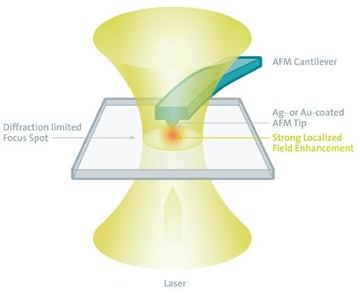
Figure 1. Working principle of TERS.
The tip radius, which characterizes the lateral resolution of an AFM measurement, is normally in the range of 10-20nm. In a TERS analysis, the lateral resolution relies on the size of the hot-spot. Hence, the expected resolution for Raman spectroscopy and imaging measurements is in the range of 20-50nm.
It is essential to illuminate the TERS tip-apex with the excitation laser from either above, below or the side. The alpha300 SR SNOM Confocal Raman combination offers the beam path geometry for all of these excitation methods (Figure 2). This article presents the results of a carbon nanowire to demonstrate the TERS capabilities of the alpha300 SR SNOM Confocal Raman combination.
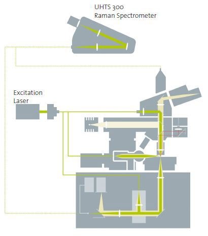
Figure 2. WITec alpha300 TERS configurations: Excitation from the side, above or below; detection from the side, above or below.
Carbon Nanowire Analysis with an alpha300 SR
Figure 3 illustrates the AFM topography image of the carbon nanowire, revealing the shape and dimension of the material. TERS measurements were carried out by bringing the tip into contact with the nanowire from above and performing the excitation (532nm) as well as detection from below. The Raman signal was acquired with a cover glass corrected 60x, 0.8 NA objective.
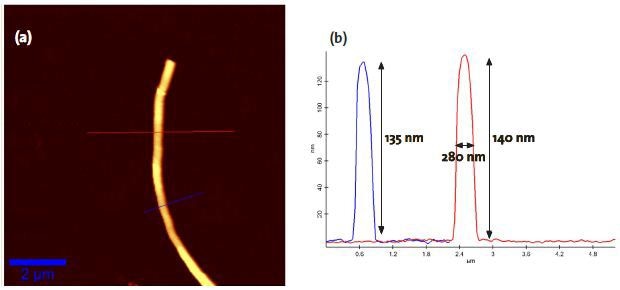
Figure 3. a) AFM topography image of the carbon nanowire used for the TERS experiments in this study. b) Data of the cross sections at the indicated lines.
Experimental Results and Discussion
The first experiment investigated the influence of general tip-induced effects to properly qualify the results acquired with the TERS geometry. The analysis involved bringing a Si/Al-coated AFM Tip into close proximity of the nanowire with no considerable Raman signal enhancement expected. Figure 4 depicts the two spectra: The red spectrum illustrates the intensity with the tip retracted and the blue spectrum delineates the intensity of the Raman spectrum with the tip in close proximity, representing an enhancement of a factor of two. As aluminum does not typically instigate enhancement, this effect might be due to mirror-like reflections (Pseudo-TERS).
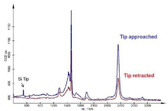
Figure 4. Pseudo-TERS effect. Raman Spectra acquired on the carbon nanowire with a Si/Al-coated AFM tip.
The second experiment involved bringing a silver-coated Si AFM tip into close proximity of the nanowire and measuring the spectral intensity (Figure 5). The blue spectrum in Figure 5 represents the spectral intensity with the tip retracted; whereas, the red spectrum represents the intensity with the tip approached. The results reveal an enhancement of up to a factor of 12, clearly showing the occurrence of the enhancement at the tip when it was in close proximity of the nanowire.
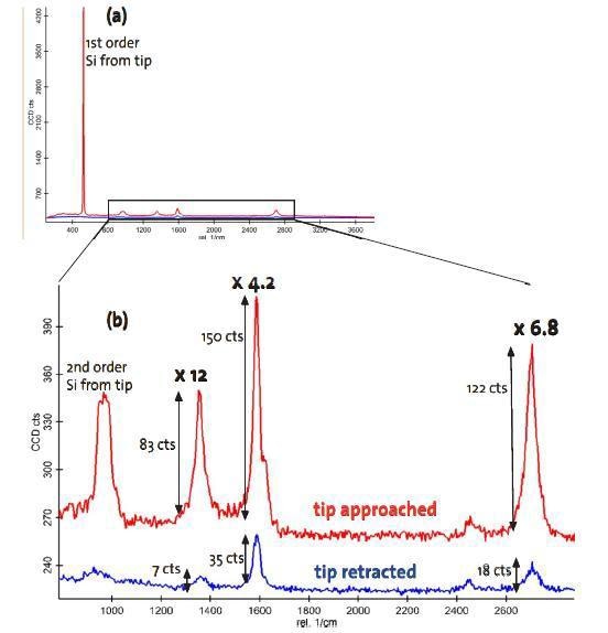
Figure 5. a) Tip-enhanced Raman spectroscopy on the nanowire. Blue spectrum: tip retracted, red spectrum: tip approached; b) Zoom-in of the fingerprint region indicating an enhancement of up to a factor of 12.
Conclusion
From the results, it is evident that the alpha300 SR is a TERS-ready system that can perform different TERS experiments, including the acquisition of single Raman spectra in TERS-mode to nano-scale Raman imaging. These results also corroborate that the alpha300 SR is ideal for chemical imaging at a resolution beyond the diffraction limit. However, various challenges need to be addressed to establish this technique as a standard and routine analysis method.
Users must be able to differentiate pseudo-TERS effects from true TERS enhancements and take measures to reduce or eliminate such unwanted effects. Availability of TERS-probes is another challenge to be addressed. More research in the field of TERS imaging and tip-functionalization needs to be carried out to establish the TERS approach as a standard and routine analysis technique for the various relevant fields of application. The TERS capabilities of the WITec alpha300 microscope series help perform such experiments.

This information has been sourced, reviewed and adapted from materials provided by WITec GmbH.
For more information on this source, please visit WITec GmbH.