Dynamic random-access memory (DRAM) is one of the fundamental units used in most of the electronic devices including smartphones, laptops, personal computers, and so on. Transistors and capacitors are the vital elements of such devices.
The FET transistor generates an access (based on gate contact signal) to the capacitor unit that is charged, thus storing the bit information. The charge on the capacitor drains gradually, hence it is essential to periodically refresh the information. Due to this fact, this memory is called dynamic.
FIB-preparation of thin TEM specimens from semiconductor devices is an important step in the physical failure analysis workflow processes executed every day in semiconductor fabrication plants. It is necessary for the lamellae to be thinned to electron-transparency with thicknesses that are compatible with the critical dimensions of the device to be analyzed; hence, nano-sized structures like transistors can be clearly resolved in the TEM.
In addition, minimal amorphous lateral damage on the prepared lamella is a fundamental requirement for TEM imaging. Low-kV polishing is an effective method for minimizing amorphous layers; however, undesirable ion implantation is another FIB-induced artifact that can interfere with or restrict TEM analysis.
Xe Plasma Source FIB
Xe plasma source FIB is an alternative for high-quality sample preparation that provides key advantages compared to more traditional Ga ion source FIBs. Such benefits include less ion implantation and the induced amorphous damage at 30 keV being lesser than that induced by Ga source FIBs. Furthermore, Xe is an inert gas that prevents the formation of metallic compounds in contrast to Ga FIBs — a property that is particularly important when it is imperative for analysis to maintain the physical properties of the sample locally unaffected due to the FIB milling.
TESCAN S9000X
The TESCAN S9000X is a plasma FIB-SEM system equipped with the iFIB+™ Xe plasma FIB column and the next generation of Triglav™, the TESCAN UHR SEM column technology. The iFIB+™ Xe plasma FIB column is an absolutely versatile sample preparation tool as it allows an extensive range of ion beam currents. On one hand, high currents allow high sputtering rates for quick removal of large-volume bulk material. On the other hand, low currents can be employed for the preparation of delicate thin TEM samples. The optimal performance of iFIB+™ at different currents is offered by a precise piezo-driven beam aperture changer for rapid switching between FIB presets and a semi-automated spot optimizing wizard with which the user can easily select the best beam spot that optimizes the FIB milling conditions for the particular application.
These features enable the preparation of good-quality TEM specimens using the TESCAN S9000X by the standard lift-out technique with — as previously discussed — added benefits with regards to the properties of Xe ions; large ion mass causes less ion implantation (in comparison with Ga at 30 keV), whereas the inert nature of Xe prevents the formation of metallic compounds that locally modify the physical properties of the sample.
While milling at low ion beam energies of <5 keV, it is possible to thin the lamellae to achieve electron transparency and thicknesses of a few tens of nanometers while maintaining least amorphous lateral damage on the lamella walls. This proves that it is certainly feasible to prepare high-quality TEM specimens using the Xe plasma FIB. The TESCAN S9000X is developed to be compatible with various in-situ analyses, which is a benefit with respect to workflow optimization and prevention of sample contamination.
EDS mapping of the prepared lamella enables the identification and location of diverse materials in the sample. EDS as a metrology tool is a technology that enables the measurement of the thickness of lamellae and thus determining whether the prepared specimens are thin enough for HR-TEM analysis. Consequently, the lamellae need not be transferred back to the FIB-SEM in case further thinning is required. This simplifies workflows in failure analysis as well as avoids sample contamination and potential sample damage during transfer. In-situ low-kV STEM imaging offers preliminary information from transmitted electrons before the robust TEM analysis at considerably higher energies. To achieve this, the TESCAN S9000X can be equipped with EDS detectors and a proprietary HADF STEM detector.
Conclusion
In this article, the preparation of a TEM specimen using the standard lift-out technique from an SDRAM memory chip based on 66 nm technology was presented. As shown in Figure 1, the sample was thinned at low-kV to a final thickness of 80 nm. Subsequently, a layer of gate contacts was exposed. In-situ STEM images in Figure 2 show 5 nm thick layers.
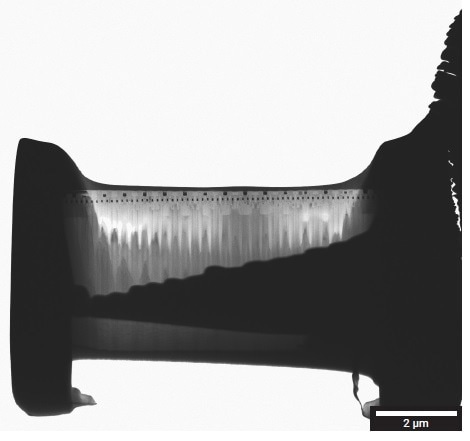
Figure 1. Overview STEM-BF image of a final lamella prepared from an SDRAM sample and polished to a final thickness of 80 nm.
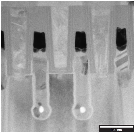
Figure 2. STEM-BF image in which 5-nm-thick layers are well-resolved.
EDS mapping was then employed to find out the elemental composition and location of the structures in the chip (Figure 3). Besides the common materials present in semiconductor devices, such as silicon, tungsten, and oxides, the thin titanium features were also well identified. The thickness of the lamellae was measured based on the EDS spectrum, showing an estimated thickness of 80 nm (Figure 4).
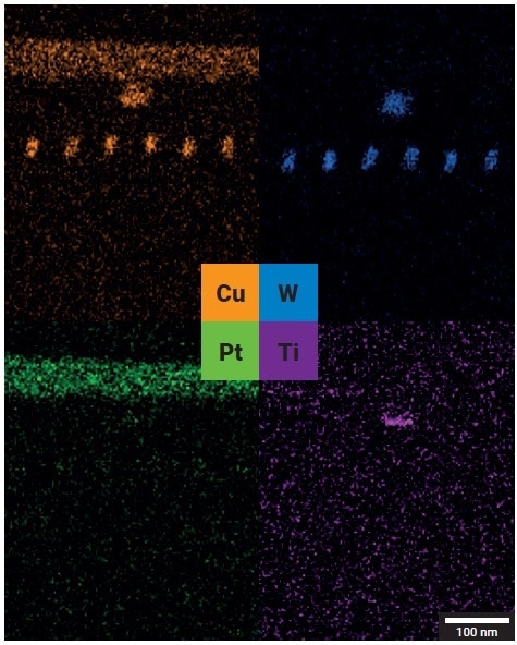
Figure 3. EDS maps showing location and composition of different elements in the chip.
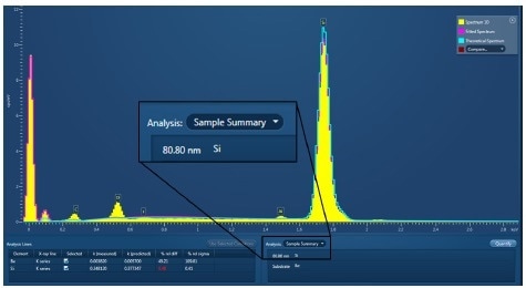
Figure 4. EDS spectrum from which a lamella thickness of 80 nm is estimated.
TESCAN Group
Founded in 1991 by a group of managers and engineers from Tesla with its electron microscopy history starting in the 1950’s, today TESCAN is a globally renowned supplier of Focused Ion Beam workstations, Scanning Electron Microscopes and Optical Microscopes. TESCAN’s innovative solutions and collaborative nature with its customers have won it a leading position in the world of nano- and microtechnology. The company is proud to participate in premier research projects with prominent institutions across a range of scientific fields. TESCAN provides its clients with leading-class products in terms of value, quality and reliability. TESCAN Group is the North American arm of TESCAN Group, a multinational company established by the merger of Czech company TESCAN, a leading global supplier of SEMs and Focused Ion Beam workstations, and the French company ORSAY PHYSICS, a world leader in customized Focused Ion Beam and Electron Beam technology.

This information has been sourced, reviewed and adapted from materials provided by TESCAN Group.
For more information on this source, please visit TESCAN Group.