|
Since the 1930’s and 1940’s many methods have been used for making electrically conductive interconnects on insulating substrates. The often conflicting requirements of cost, electrical insulation, thermal management, track definition, track adhesion, signal transfer speed, current-carrying capability, resistance to adverse working environments, physical strength, performance at high frequencies and so on, have meant that varying degrees of success have been achieved. However, during the last few years the process of copper-plating ceramic has been greatly improved. It can now be considered as a serious alternative to well-established interconnect methods such as etched Cu/epoxide-glass laminates, ‘screen-and-fire’ thick-film circuits, evaporated-metal-on-glass thin-film circuits and etched thick-film.
Copper-Plated Ceramics
Copper-plated ceramic addresses the interconnection requirements of many of the latest electronics systems. The key features stem from the combination of the insulator, the conductor and the manufacturing methods.
Materials and Sizes
The normal insulator used is 96% alumina ceramic. When the highest performance at frequencies above 5GHz is required, 99.5% alumina is used, but since the prices differ by a factor of ten, it is used only when applications require lower losses at higher frequencies. Individual circuits can be produced in any size up to the dimensions of the ceramic panel used, usually 100mm x 100mm or 150mm x 100mm. If more than one circuit fits on to the panel, they are usually made in multiples, with each circuit printed onto prescribed section.
Why Use Alumina for the Insulator?
The electrical properties of alumina are excellent. The insulation resistance is very high and, over the range that affects circuit boards, does not change significantly with either temperature or humidity. The thermal conductivity is reasonable, being a little under one tenth that of copper but around one hundred times that of most organic materials.
Why Use Copper for the Conductor?
The conductor is pure electroplated copper. For all practical purposes only silver has higher electrical conductivity, but copper is cheaper, much more metallurgically stable and its solderability, regarding tin-lead solders, is very well understood. Conductor thickness can range between 5μm and 100μm with only a minimal additional cost for higher thickness. At the highest thickness some loss of resolution capability occurs - the ultimate resolution is mainly limited by the surface quality of the substrate. The conductors have near rectangular cross-sections, very low surface area to volume ratio and the top surface of the conductor is as smooth as that of the substrate. The electrical resistance of the tracking is about 1 milliohm per square for a thickness of 25μm
Other Materials
Despite the fact that pure copper is eminently suitable for solder assembly, it is often necessary to add other materials for various reasons, such as:
• Preventing oxidation during storage, aesthetics, wirebonding and protection against solder-bridging and physical damage
• Organic anti-tarnish coatings prevent oxidation and discolouration by sulphur-containing gases. Plated gold (sometimes over plated nickel) is used both for aesthetics and where wire-bonding is contemplated
• Tin-lead can give retention of solderability during longer storage periods
• Photo-imaged solder mask minimises solder‑bridges and physical/handling damage
• Electroless silver is also available.
These finishes may cover the entire circuit or can be applied only in selected areas.
Performance of Copper-Plated Ceramic Circuits
Concerning the reliability of copper-plated ceramic circuits, a number of tests similar to those carried out on thick film circuits have been made and, in general, the overall performance has been found to be equivalent or superior to conventional thick film. Adhesion of conductors is excellent and, when using a nail head pull test, it is normal for either the wire or ceramic to break, even after ageing at 150°C.
When assessing reliability it is important to relate the test to the technology. For example, the specification for a biased damp-heat test needs to take account of the fact that the electric field between two tracks 50μm apart is much higher than for two tracks 250μm apart for the same applied voltage.
Table 1. Comparison of various circuit technologies.
|
|
|
Track resolution
|
50
|
250
|
150
|
150
|
|
Track resistivity
|
1-2
|
10-30
|
2-4
|
5-10
|
|
Solderability
|
Outstanding
|
Good
|
N/a
|
Very Goog
|
|
Wire-bonding Au
|
Yes
|
?
|
Yes
|
Yes
|
|
Wire-bonding Al
|
Yes
|
Yes
|
Not pure gold
|
Yes
|
|
Unit costs
|
Low
|
Low
|
High
|
Low
|
|
Tooling costs
|
Low
|
Low
|
Low
|
High
|
Economics of Materials Selection
If the needs of the particular application can be met by standard processing of FR-2 or FR-4 laminates, it is unlikely that the benefits of copper-plated ceramic will justify the higher cost. However, if the use of other types of expensive base-board materials such as PTFE-glass or glass-silicone is being contemplated, then it is probable that a very cost-effective solution can be found by choosing copper-plated ceramic.
When compared with single-layer silver thick-film circuitry, copper-plated ceramic gives a broadly similar cost. However, if more than one layer is required in thick film or if gold-based conductors are required, then copper-plated ceramic will almost certainly be cost-effective.
Features and Advantages of Copper-Plated Ceramic Circuits
Features, advantages and benefits can be summarised as follows:
• Higher circuit density than conventional FR-2, FR-4, PTFE, polyimide, thick-film and co-fired ceramic circuits
• Outstanding high-frequency characteristics
• Excellent thermal management and heat-transfer performance
• Outstanding solderability and wire-bonding assembly characteristics
• Low tooling costs and quick turnaround of prototypes.
System Design
A key step in the design of many electronics systems is to divide the system into sub-modules which can be independently assembled and tested. A major benefit of the `modular' approach is that the best available assembly technique can be used for each module, which can then, together with others, be comparatively easily assembled on to relatively simple boards, exactly the right combination for minimising costs and optimising performance.
Interconnects for Modules
Several possible techniques are available for interconnecting such modules, for example, high-density plated copper is useful in a number of applications. It is more versatile than the so-called ‘silicon hybrid’ but cannot achieve the interconnect density afforded by this thin-film method.
The costs per unit area associated with copper-plated ceramic are believed to be lower than for ‘silicon hybrid’, particularly as plated-ceramic may not need additional packaging and the track-resistance is lower.
Where Copper-Plated Ceramics Have Advantages
Situations in which copper-plated ceramic is advantageous include:
• Where the module requires both ‘chip-and-wire’ and solder assembly, particularly when ceramic chip-carriers and chip-capacitors are involved. Selective-plating of the copper gives excellent wire-bonding characteristics and the combination of bulk-metal and substrates with good thermal conductivity leads to outstanding solderability. The ability to make 50μm-wide tracks allows wire-bond sites to be placed close to semiconductor devices, which is a key benefit when comparisons are being made with thick film and co-fired ceramic
• When TAB (tape-automated bonding) is contemplated. The copper tracks are finished with plated tin-lead, enabling multi-lead connections as fine as 100μm track and gap to be soldered without the formation of solder balls or solder bridges
• Where additional packaging is not wanted. It is quite possible to use the assembly with just the attachment of a lead-frame (and maybe plastic encapsulation for the wire-bonded devices)
• If film (printed) resistors are required but in combination with one or more of the other benefits mentioned.
|
|
|
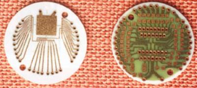
Figure 1. High Density module. Additional packaging is rarely needed.
|
The technology enables patterned conductors to be added to both sides and also to the edges of substrates. Solder bumps have also been added to substrates by the selective plating of tin-lead. Bumps as small as 50μm on a 100μm pitch suitable for flip-chip bonding have been produced.
Summary
Overall, the take-up of this technology has been impressive - more than fifteen million copper-plated ceramic circuits are now in service, with the six hundredth design completed recently. Moreover, every twelve seconds, somewhere in the world a system is assembled which takes advantage of this technology.
|