Curtaining is a common problem encountered when using a focused ion beam (FIB) method to prepare TEM lamella. Curtaining is the result of non-uniform thinning of the sample, and presents itself as a roughness on the sample edge. This effect impacts the quality of the following analysis and the quality of the images taken.
Curtaining is often present when the sample is heterogeneous, i.e. produced from different materials, as this can result in variable thinning rates. This article will explore reducing the extent of curtaining by changing the direction of ion beam thinning/polishing of the sample using the OmniProbe 400 nanomanipulator’s rotating function.
Curtaining is at its most extreme when the sample consists of a hard material, which is milled slowly, above or inside a soft material, which is milled quickly. This is often the case in semiconductor failure analysis, though is also present in many other applications. In these instances, the best milling geometry is thinning from the anterior side of the sample (backside thinning).
This article will show how backside thinning, using the OmniProbe 400 nanomanipulator and OmniPivot holder, can be used to prevent curtaining. The article will also demonstrate how time can be saved by assessing lamina quality in the machine using the AZtec® LayerProbe.
Sample Preparation
To carry out backside thinning a number of steps must be carried out (Figure 1), with the repositioning of the TEM grid and the rotation of the probe being the most important parts.
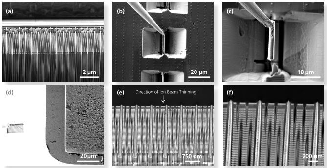
Figure 1. Steps in the production of a backside thinned TEM lamella. The lamella is prepared by conventional milling (a), the sample is then rotated (b) and the lamella lifted out (c). By rotating the probe, the sample is angled 90º relative to the ion beam (d). The complete 180º rotation is achieved by pivoting the grid to 90º which allows backside thinning (e) and removes curtaining (f). It is important to note that the rotations used is dependent on the probe take off angle (TOA) and there are multiple combinations for a given instrument.
The OmniProbe 400 is port mounted, meaning it has a constant manipulator take off angle allowing the required rotation of the probe to be determined. In addition, the probe’s compucentric rotation means that the rotation can be carried out rapidly without problems.
The TEM grid can be repositioned using the OmniPivot grid holder, which reduces risks associated with direct manipulation of the grid.
Advanced Thinning
The sample shown in Figure 1 is a 3D NAND flash device, such as those found in commercial solid-state hard drives, which has wordlines and W slits embedded in a silicon substrate. A control sample was also taken from the same device which was thinned using a conventional method at the same milling parameters. Figure 2 compares the lamellae of both samples to demonstrate the benefits of backside thinning.
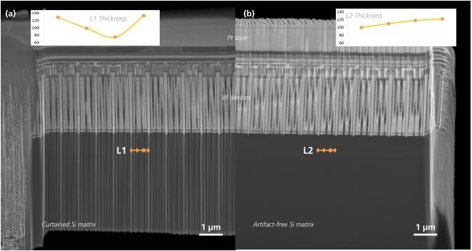
Figure 2. (a) Lift out sample prepared from the 3D NAND Flash device by conventional thinning. The thickness profile L1 measured in the Si matrix shows large, sudden changes in thickness; (b) Backside thinned liftout of the same device using the same FIB conditions. Thickness profile L2 taken from the Si matrix shows a smooth and uniform lamella thickness.
The thickness of the silicon substrate was determined using the AZtec LayerProbe, and this value was used to determine the extent of thinning. This process was carried out via EDS and repeated between milling steps, with a line of EDS points used to determine the thickness.
It was observed that the lamella prepared using a conventional method are rough with random thickness variations of approximately 60 nm, whilst the samples prepared using backside thinning has a smooth surface with no random variation.
Conclusion
Producing lamella for TEM analysis can be a rate-limiting step in failure analysis because multiple FIBs may be needed to support one TEM system.
This article has shown that fast backside thinning of lamella is possible using the OmniProbe 400 nanomanipulator and the OmniPivot holder. This process can be monitored using the AZtec LayerProbe to determine the lamella thickness, ensuring that the lamella are of sufficient quality prior to TEM analysis.

This information has been sourced, reviewed and adapted from materials provided by Oxford Instruments NanoAnalysis.
For more information on this source, please visit Oxford Instruments NanoAnalysis.