SilcoTek is located in Bellefonte Pennsylvania and is only a few miles away from the main campus (University Park) of Penn State University. It has transformed this geographic proximity into a strong collaborative relationship with a world-class research institute.
The R&D scientists at SilcoTek are all trained users of the University’s Materials Characterization Lab (MCL). This lab has a wide variety of characterization techniques and equipment as well as a group of experienced staff scientists who are available to answer questions related to materials science. The following sections will focus on a few techniques that a frequently used by scientists at SilcoTek through Penn State University. Other than those discussed below, SilcoTek also has access to all the techniques listed on PSU MCL’s website.
Scanning Electron Microscopy (SEM)
The scanning electron microscope was developed to allow a “closer” look at a material when the optical microscope cannot provide adequate resolution at the detail levels needed. The SEM has overcome two intrinsic limitations that hinder the traditional optic microscope: poor depth of field and low resolution5.
Theoretically, the highest resolution of an imaging technique is the size of half of the wavelength of the imaging energy. SEM uses electrons rather than visible light (as in an optic microscope) as the imaging source. Since the wavelengths of electrons are orders of magnitude lower than that of visible light, SEM can achieve a significantly higher resolution than the optical microscope.
Depth of field is limited in the optical microscope due to its large aperture angle at high power objective lenses (short focal lengths increase the aperture angles). However, an SEM has a long working distance and a very small aperture angle and so can provide a much better depth of field.
In an SEM, a focused beam of electrons impinges upon a specific area of the sample specimen in a raster pattern. The incident electrons can take one of three pathways:
1) they can have an inelastic collision with an electron in the sample atom and create secondary electrons (energy < 50 eV)
2) they can experience elastic collisions (i.e. no loss of kinetic energy) with the nucleus of the sample atoms and create backscattered electrons (energy > 50 eV)
3) they can pass through the space within the sample without any collisions. Appropriate detectors can be used to collect either backscattered or secondary, electrons emitted from the sample surface and then process them into images. These images are then projected onto a cathode ray tube (CRT) that can be seen.
The secondary electron (SE) imaging mode typically provides excellent surface topographical contrast whereas the backscattered electron (BSE) imaging mode highlights the density differences in the sample.
Penn State’s MCL has a number of SEM instruments that offer beam deceleration or low vacuum operation mode, producing resolutions down to sub-nanometer scale with the latest tool addition.
Figure 9 below shows SEM images of the surfaces of two SilcoTek coatings (taken in SE mode), where R&D scientists have experimented with ways to control the coatings surface topography (smooth vs. rough).
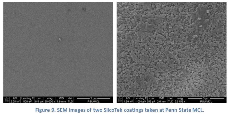
SEM benefits SilcoTek customers by: providing the visual characteristics of coatings at very high magnifications; highlighting surface imperfections and assisting in troubleshooting.
Energy-Dispersive X-ray Spectroscopy (EDS)
EDS is an elemental analysis technique and is usually installed in electron column instruments such as the SEM. Therefore, it is often used in conjunction with SEM and referred to as SEM-EDS.
Secondary electrons are knocked out of their shells when the incident electron beam in an SEM bounces through the sample. These secondary electrons are collected by a detector to form an SEM image) and leave behind thousands of vacant shells in the sample atoms. Having a vacant inner shell causes the atom to become unstable and an electron from a higher energy outer shell will drop into the vacant inner shell to fill the “hole.”
This process releases the energy difference between the two shells in the form of an X-ray emission. The wavelength and energy of the X-ray is unique to each element as well as to the shells involved (e.g. a Ka line refers to the X-ray emitted as a result of an L-shell electron filling a vacant K-shell). As a result, collecting and analyzing these characteristic X-ray lines allows the sample’s elemental composition to be resolved.
Since the X-ray emission comes from the same sample area where the electron beam strikes, the area that is being imaged (in an SEM) is the same area that is being analyzed by EDS. Depending on the sample density and the energy from the incoming electron beam, the EDS depth of information is usually from 0.5 to 3 mm.5
EDS is therefore considered as a bulk elemental analysis technique and does not provide adequate resolution to the top tens of nanometers of a surface. Various analytical models can be employed in an EDS measurement including mapping of the elements, elemental line scans and spectrum acquisition.
Figure 10 below shows the SEM-EDS analysis results of an aluminum substrate with silicon dioxide (SiO2) contamination, performed at Penn State University’s MCL. The different elements were highlighted in different colors using the elemental mapping mode. Scientists at SilcoTek used this technique to rapidly identify the contamination species on an aluminum substrate during a troubleshooting process.
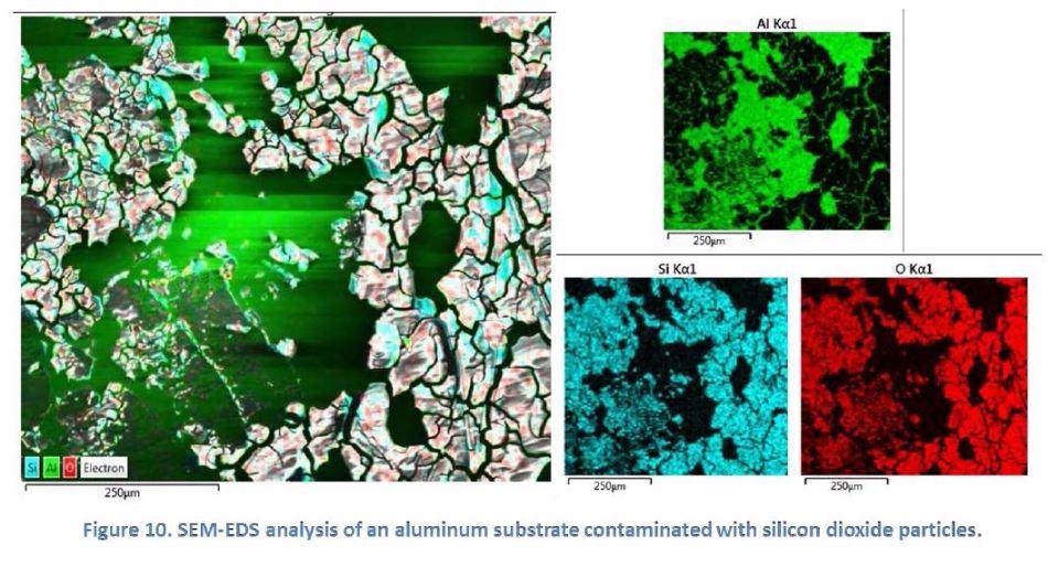
EDS benefits SilcoTek customers by providing elemental analysis information and assisting in troubleshooting.
X-ray Photoelectron Spectroscopy (XPS)
One of the most useful surface sensitive analytical techniques available today is XPS. It can detect all elements aside from helium and hydrogen, and it offers a depth of information from the top 1 to 10 nm of the surface region of a sample.5
In XPS, an incoming X-ray beam bombards a sample surface and its energy gets absorbed by the sample atoms in the surface. If the energy of an X-ray photon is enough to free an electron from its nucleus then the escaped electron (known as a photoelectron), will emit out of the sample surface. According to Einstein’s photoelectric law, the incoming photon’s energy is split into two portions: one is used to overcome the electron’s binding energy (BD) and free the electron from its core, and the remaining portion is transferred as kinetic energy to the photoelectron.
Since the energy of the incoming X-ray photon is known, measuring the kinetic energy of the photo helps to determine the value of BE. The BE is characteristic of the specific element but also of its chemical state and the binding environment of those elements. The intensity of the photoelectrons can therefore be used to determine the relative concentrations of each element.
Figure 11 below demonstrates the use of XPS in the PSU MCL to study the oxidation process in a coating. Scientists at SilcoTek use this technique to study the oxidation of the silicon atoms in a coating, demonstrated by the binding energy shift from Si-C to Si-O.
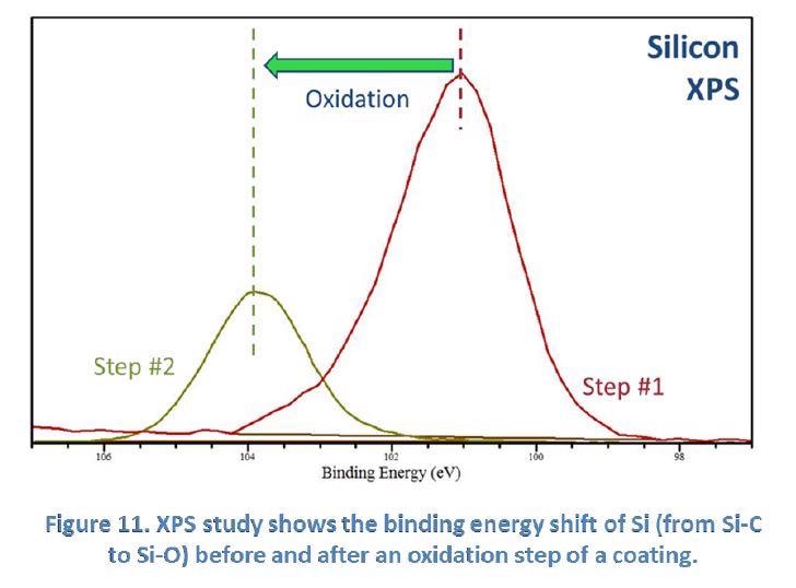
XPS benefits SilcoTek customers by providing true “surface” (top 1-10 nm) information; confirming successful surface bonding; identifying surface contamination and detecting surface chemical changes.
Dielectric P-E Measurement
Customers are increasingly inquiring about the electrical properties of SilcoTek coatings. Generally, SilcoTek’s silicon-based coatings (SilcoNert® and Silcolloy®) exhibit resistor-like behavior (i.e., they allow electric current to flow through them). Conversely, Dursan is a dielectric coating (i.e., an electrical insulator that gets polarized by an applied electric field and through the polarization stores electricity).
Characterization of SilcoTek coatings’ dielectric properties is performed at the Dielectric Properties Lab at Penn State MCL using a P-E (polarization vs. electric field) measurement. A P-E loop is a plot of the charge or polarization (P) developed against the field (E) applied to that device at any given frequency.
The P-E loop for a linear capacitor is ideally a straight line whose gradient is proportional to the capacitance. However, if there is current leakage through resistive losses (also known as a lossy capacitor), the straight line will open up into a narrow loop. This indicates resistive leakage in the device.
Figure 12 below shows the P-E responses of two Dursan coatings. The left graph shows what would be described as a “lossy capacitor” whereas the right graph shows the linear P-E response of an ideal dielectric coating with low loss. SilcoTek scientists have used this characterization tool to develop process improvement and to eliminate the “lossy capacitor” response towards a good dielectric coating.
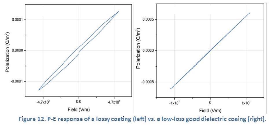
P-E measurement benefits SilcoTek customers by providing dielectric property information and detecting current leakages in coating.
Summary
This article gives a brief overview of a range of material characterization techniques available to SilcoTek. It aims to help customers understand the scope and capability of SilcoTek’s R&D activities and to illustrate how different tools can be used to facilitate SilcoTek in developing more innovative solutions to help customers solve various application challenges.
The easy availability of these tools allows the manufacturing team at SilcoTek to keep tight quality control on coating products. Consequently, SilcoTek can provide consistent and reliable coating services to all customers.
Furthermore, the close ties SilcoTek has with Penn State University means access to some of the most advanced characterization equipment/techniques available. SilcoTek’s goal is to convert that advantage into provision of the best coating services and solutions possible for customers.
References
- Y. Yuan and T. R. Lee, “Contact angle and wetting properties”, Surface Science Techniques 2013, DOI 10.1007/978-3-642-34243-1_1.
- P. Roach, N. J. Shirtcliffe and M. I. Newton, “Progress in superhydrophobic surface development”, Soft Matter 2008, 4, 224.
- Y. Zuo, R. Pang, W. Li, J. P. Xiong and Y. M. Tang, “The evaluation of coating performance by the variations of phase angles in middle and high frequency domains of EIS”, Corrosion Science 2008, 50, 3322.
- Gamry Instruments Application Note “Basics of electrochemical impedance spectroscopy”.
- C. R. Brundle, C. A. Evans Jr. and S. Wilson, “Encyclopedia of materials characterization: surfaces, interfaces, thin films”, Butterworth-Heinemann, 1992.
This information has been sourced, reviewed and adapted from materials provided by SilcoTek.
For more information on this source, please visit SilcoTek.