This article will discuss why SilcoTek specify a CVD coating thickness range rather than a specific thickness.
Firstly, this article will review the chemical vapor deposition (CVD) coating process.
This article will cover:
- How the part surface can impact coating thickness variation
- The sources of coating thickness variation in silicon CVD processes
- Which tools are used to characterize a surface for optimum coating quality
- How the coating reaction rate can impact thickness
Chemical vapor deposition is a process that involves the reaction of a volatile precursor which is injected into a chamber, typically under a vacuum. The chamber is heated to a reaction temperature and this causes the precursor gas to react or to break down into the desired coating and then bond to the material surface.
As time passes, the coating material builds on the surface and creates a coating throughout the surface of the exposed part.
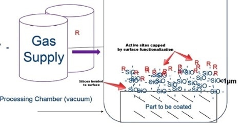
The chlorine and hydrochloric acid gas will be vented from the chamber and scrubbed according to appropriate regulatory requirements whilst the silicon will bond to any exposed surfaces (both internal and external). The CVD coating system may look similar to the diagram below. In this example, the desired coating material is a silicon oxide base coating with a functionalized (R) surface. The surface is indented to cap any remaining active sites on the coating surface, making it a superior non-reactive surface.
The CVD process differs from physical vapor deposition (PVD) which involves vaporizing a coating material and then spraying or condensing the vaporized material on the surface. This causes a line of sight application rather than the non line of sight application that is achieved with CVD. The graphic below shows what coated parts would look like.
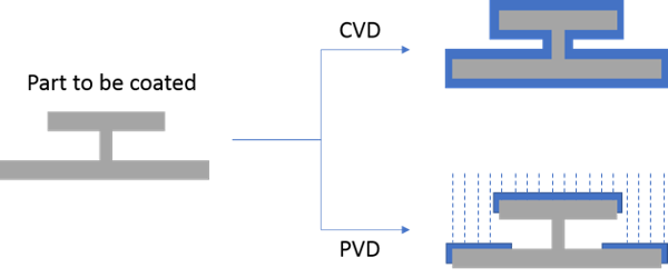
With PVD, surfaces must be exposed to the application vapor because shielded areas will not be coated. A good analogy is that of snow covering garden furniture. There will be little snow under the furniture whilst there will be a lot on the top of the table.
On the other hand, chemical vapor deposition will react and apply to any area that the coating gas can get into. This deposition process allows the application of a silicon layer on the surface one Angstrom (0.1 nanometer) at a time. Theoretically, it should be possible to specify the thickness of the coating to the nanometer, so why do CVD coatings have a thickness range? Practically, variation and process limitations result in specifying a range of coating thickness.
Sources of Variation in the Coating Process
The table below summarizes the range of coating thickness for each of the SilcoTek coatings. This difference in thickness is due to multiple contributing factors that add up to variation in the thickness of the coatings.
| |
SilcoNert® 1000 |
SilcoNert® 2000 |
Dursan® |
Silcolloy® |
SilcoKlean® |
SilcoGuard® |
Dursox® |
| Thickness range (nm) |
100-500 |
100-500 |
400-1600 |
180-800 |
100-500 |
180-600 |
400-1600 |
Below are a few of the contributing factors that add to variation in CVD coating thickness and thickness specifications.
Part Surface
How do you know if a part is electropolished to a mirror finish with little surface roughness (5 ra for example?) or cast with a very rough surface? Using the snow analogy, with the part surface being a mountain range, as the snow falls on the mountains it covers the valleys more heavily than the cliffs. The SilcoTek coating process coats the entire part but may preferentially coat some areas of rough surface.
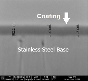
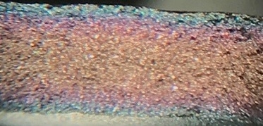
There is not a large amount of variation but the surface does contribute. The SEM image below is a good example: some changes in part surface (light gray) and the impact on the overall coating thickness can be seen. Over the small area of the sample surface you can see 8 nm in thickness variation.
Part Configuration
The SilcoTek process will coat the interior of a part as well as the interior. The coating volume available can play a role in coating thickness. A small and confined area, like the interior bore of a needle, tends to have slightly less coating available to bond to the surface. SilcoTek has a few methods to minimize the effect but in some parts, the configurations of the coating thickness may change.
This is especially true in extremely narrow bores, blind holes or within fritted metals like the photo below. The section of the fritted filter shows a band of color which indicates variation in coating thickness from the interior to the exterior of the filter surface. Color is generally an indicator of coating thickness and this will be discussed later.
Base Material and Surface Condition
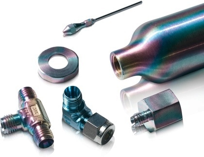
SilcoTek mostly coats stainless steel alloys but can also coat ceramics, glass and more exotic alloys like titanium. Under certain conditions the base material can affect the coating rate and add to variation. Furthermore, if the base material surface is heat stained, etched, oxidized, scratched or buffed the coating thickness in those areas can vary.
Coating Reaction Rate
Most CVD reactions are driven by heat. During processing there is usually a point at which the ideal temperature vs. the coating growth rate is achieved. Given the right amount of heat it is theoretically possible to build a 1000 nanometer coating in a few seconds or with a minimum of heat build a layer over a few days or months. If a lot of heat is applied, the reaction is driven very fast and it is hard to stop a fast reaction in a quick and precise way.
A fast reaction also means it is more likely that the target layer thickness will be overshot but a slow reaction may not necessarily be better. If the process is too slow it will add significant processing time and cost. Theoretically it is possible to specify a coating to the nearest tenth of a nanometer at a very low heat reaction.
However, few customers are willing to wait the weeks or months necessary to slowly build a coating layer in a low heat reaction.
The ideal CVD balances process cost, time and coating thickness variation. The process SilcoTek uses has optimized time, cost and value for the customer without impacting coating performance. SilcoTek has spent thousands of hours evaluating and then optimizing coating performance for each industry application.
Optimization involves trade-offs between performance and process. These trade-offs happen all the time in surface finish operations, machine shops and in nearly all products made today.
A user would not notice the difference between a 500 nm and an 800 nm coating for paints or other coatings. SilcoTek customers notice minor thickness variation in the silicon coatings because the coating color changes with even a small variation in thickness.
What Does SilcoTek Variation Look Like?
SilcoTek bonds silicon to glass, ceramics or metals through the process of CVD and this process enables the building of a silicon layer on a surface on Angstrom (0.1 nanometer) at a time. A very thin layer of silicon is so clear that it is see through. As the silicon thickness increases, e.g., on a stainless steel surface, the light which travels through the silicon is bent. Then the light reflects off the stainless steel surface and is bent again.
This bending of the light causes some wavelengths of light to cancel out each other but some wavelengths are reinforced. The reinforced wavelengths hit the cones in the eye and are seen as color whilst the canceled (or interference) wavelengths cannot be seen. Changing the color of a thin silicon surface is easy, a few nanometers change in silicon thickness can have a big impact on the colors you see.
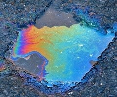
A good analogy is that of oil on water. After a rainstorm a colorful rainbow oil slick can be found on surface oil. Oil is not normally colorful, it is either honey colored or black (as it gets older). The black becomes a colorful rainbow because of refraction. Light reflects off the surface of the oil and also travels through the thin oil and is reflected back from the water surface below the oil.
Depending on the thickness of the oil, light rays are either reinforced or interfered with by the oil refraction. As the rays of light reach the eye, the destructive interference wavelengths cancel each other out. The oil thickness variation dictates which colors are seen and which color wavelengths are canceled out. This analogy demonstrates that a slight variation in thickness can have a big impact on the color that is seen.
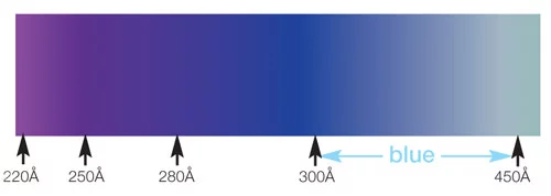
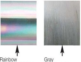
Small variations in thickness can also make a big difference in the color of the silicon coating. The differences in the colors observed on SilcoTek treated parts indicate different layer thickness. A blue color indicates a 300 to 450 Angstrom layer while a rainbow color corresponds to a coating of at least 1200 Angstroms (120 nanometers).
Depositions used in the SilcoGuard® and Silcolloy® processes are up to 1 mm (1000 nm) and have a rainbow to silver/metallic gray appearance. The images below show colors created by Silcolloy®, an 800 nm** coating (right) and SilcoNert®, a 500 nm** coating (left). A few nanometers change in thickness will result in a dramatic change in the color of the part.
Which Tools are Used to Characterize a Surface for Optimum Coating Quality?
Material surface characterization capabilities play an essential role in supporting SilcoTek® coating science and R&D efforts. Being able to thoroughly evaluate a surface is important for developing new inert barrier coating products, and has a key role in assisting customers with troubleshooting and scale up.
Many surface characterization techniques allow scientists at SilcoTek to study materials, analyze surface bonding mechanisms and develop a deep understanding of surface properties. Production technicians at SilcoTek® use material characterization tools in their daily QA/QC process to ensure all inert, corrosion resistant coatings meet the quality standards and satisfy the customer.
Finally, customers often work with R&D staff to provide characterization help with specific substrates or coated parts as a part of product development.
As well as the capability for in-house characterization, SilcoTek® also has access to a wide range of characterization techniques at the Pennsylvania State University (PSU). This is due to the physical proximity of SilcoTek to the main campus of the University and also an established academic/industry relationship between PSU and SilcoTek. The R&D scientists at SilcoTek are certified users of many characterization instruments, for example scanning electron microscopes (SEM) which are located at the Materials Characterization Lab (MCL) at Penn State University. Here are some of the tools that SilcoTek uses to support customers, products and processes.
Which Tools are Needed to Characterize a Surface?
Coating surface characterization begins with a knowledgeable and capable R&D team. The tools used to help analyze the surface vary with application and need. Below are a few tools used at SilcoTek to understand CVD coatings and surfaces.
X-ray Fluorescence (XRF) Analyzer
SilcoTek uses a Thermo Scientific X-ray fluorescence (XRF) analyzer to avoid process disruptions caused by incompatible substrates. This is a non-destructive elemental analysis tool which identifies any unfamiliar incoming metal substrates.

This is important because the substrate material affects the surface bind, coating quality and ultimate product performance. Knowing the base material means that the SilcoTek process technicians use the most appropriate processing methods in order to get the best coating results possible.
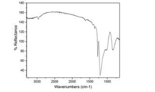
Fourier Transform Infrared Spectroscopy (FTIR)
FTIR uses a broad band infrared radiation as the excitation source to probe molecular structures of multiple chemical species in either gas, liquid or solid state. FTIR is regularly used by the technicians at SilcoTek to perform QA/QC duties and also by scientists to assist in their R&D projects.
This is important because FTIR can be used to determine surface quality on a molecular level. It can also be used as an additional tool in combination with visual inspection criteria in order to better assess coating quality.
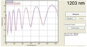
F20 Thin-Film Analyzer
The F20 Thin-film analyzer is a bench top tool and can be configured to measure thin film thicknesses from 30 Å to 350 mm. It can also measure optical constants such as a refractive index, extinction coefficient and transmittance. SilcoTek uses it primarily as a quick, accurate and non-destructive way of measuring surface thickness and assuring consistent coating quality.
Surface Contact Angle Measurement
Contact angle is the angle that a drop of liquid makes to its, usually solid phase, contacting surface. It is measured through the droplet and the angle is formed between the solid surface and the liquid meniscus near the line of contact. This measurement gives an indication of the wettability of a surface to a liquid (usually water).
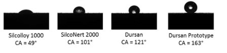
Scientists at SilcoTek rely greatly on the contact angle measurement in their research of hydrophobic and superhydrophobic surface development because properly designed surface energy can bring out the extreme water-repellent property in a surface or it can prevent surface fouling or enhance mold release.
Contact angle measurement benefits SilcoTek customers by making sure that the anticipated surface energy (hydrophobicity/hydrophilicity) required by the application is achieved.
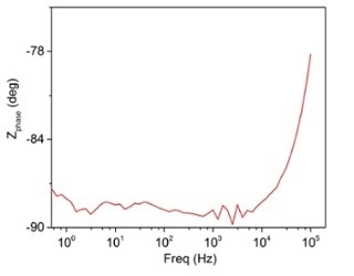
Electrochemical Impedance Spectroscopy (EIS)
EIS is a very useful and mostly non-destructive tool used to study and evaluate the performance of protective coatings on metal substrates. This measurement gives information on capacitance, resistance, double layer capacitance and Faradaic impedance, all of which are related to the performance and failure process of coatings. They are especially important during corrosion resistance testing. EIS helps the engineers and scientists at SilcoTek to identify coating pinholes and to develop better and more uniform coatings.
This article highlights a range of materials characterization techniques that are used by SilcoTek®. It aims to help SilcoTek customers to understand the scope and capability of R&D activities and also to demonstrate how different tools can be used to facilitate SilcoTek in the development of more innovate solutions and solve customer application challenges.
The easy availability of these tools allows the manufacturing team at SilcoTek to ensure tight quality control on the inert coating products and provides consistent and reliable products to all SilcoTek customers.
This information has been sourced, reviewed and adapted from materials provided by SilcoTek.
For more information on this source, please visit SilcoTek.