Nanowires are of great interest because of their promising electronic and optical properties, which make it possible to manipulate light. These nanostructures have confinement effects and novel physical properties that are not otherwise exhibited in bulk materials.
Of special interest are nanowires based on group-III nitrides such as GaN since they are semiconductor materials with a wide band gap, a property which has made it possible to envisage far reaching applications in modern micro- and optoelectronic devices including laser for lighting, sensors, and flexible optical devices such as displays.
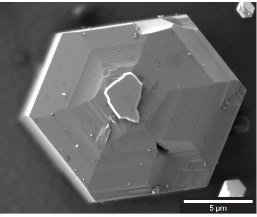
It has been found that physical features such as length, diameter, alignment, composition, crystalline structure, purity, doping, defect density, as well as growth direction and nature of facets are all essential in determining the emission and absorption properties of nanowires, and therefore in determining their use and applications.
For instance, when the nanowires are grown vertically aligned with respect to the surface substrate, light can escape only at the top facet while the light emitted from sidewall facets would be absorbed by surrounding rods. Such nanowire arrays are suitable for photovoltaic devices.
 Want to know more? Click here to read the full article
TESCAN Group
Founded in 1991 by a group of managers and engineers from Tesla with its electron microscopy history starting in the 1950’s, today TESCAN is a globally renowned supplier of Focused Ion Beam workstations, Scanning Electron Microscopes and Optical Microscopes. TESCAN’s innovative solutions and collaborative nature with its customers have won it a leading position in the world of nano- and microtechnology. The company is proud to participate in premier research projects with prominent institutions across a range of scientific fields. TESCAN provides its clients with leading-class products in terms of value, quality and reliability. TESCAN Group is the North American arm of TESCAN Group, a multinational company established by the merger of Czech company TESCAN, a leading global supplier of SEMs and Focused Ion Beam workstations, and the French company ORSAY PHYSICS, a world leader in customized Focused Ion Beam and Electron Beam technology.

This information has been sourced, reviewed and adapted from materials provided by TESCAN Group.
For more information on this source, please visit TESCAN Group.