The usual workflow for physical failure analysis involves delayering with chip deprocessing and defect isolation using electrical characterisation such as nanoprobing and conductive AFM, followed by defect characterisation through visualisation and material analysis in TEM.
The deprocessing and electrical characterisation steps in the workflow still employs multiple tools. Conventional deprocessing techniques are coarse, lack localised precision and has a rough final surface thus site-specific deprocessing and electrical characterisation is now achievable with a single workhorse, the TESCAN S8000X plasma FIB-SEM. Of all the things, producing a high degree of planarity (under 5 nm RMS surface roughness) for easy accessibility of the nanoprobes and with minimal foreign ion implantation that can change the electrical properties of the device are the most critical. High-resolution imaging delivered by the BrightBeam™ SEM column enhances very low keV imaging and sheds light on defective lines with passive voltage contrast (PVC). High resolution live imaging at 200 eV/500 eV with currents under 40 pA and Kleindiek’s Probe Shuttle PS8 in-situ nanoprobing capabilities come in handy for measuring I-V characteristics in-situ which explains the measure of defect or functionality in unit structures like PMOS and NMOS transistors in sub-20 nm devices.
The TESCAN S8000X is a dual-beam instrument fitted with the SEM column BrightBeam™ SEM with outstanding ultra-lowkeV imaging capabilities (with 500 and 200 eV beam energies and 40 pA beam currents) – without using beam deceleration –, and the new iFIB+™ Xe+ plasma FIB with a wide range of beam energies (30 keV to 3 keV) and range of currents (1 pA to 2 μA) to encompass multiple application base. Xe+ plasma FIB-SEM system fits perfectly for some key semiconductor failure analysis applications – one of them being delayering.
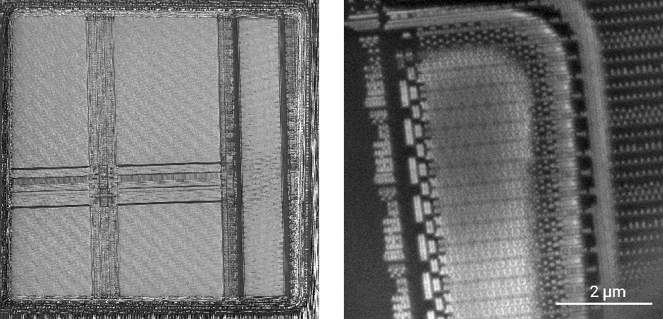
Gas-assisted delayering of a 10 nm node process with Xe plasma FIB. (Left) Overview of a 100 × 100 μm² delayered window (Right) Layer of interest imaged at 200 eV.
 Want to know more? Click here to read the full article.
TESCAN Group
Founded in 1991 by a group of managers and engineers from Tesla with its electron microscopy history starting in the 1950’s, today TESCAN is a globally renowned supplier of Focused Ion Beam workstations, Scanning Electron Microscopes and Optical Microscopes. TESCAN’s innovative solutions and collaborative nature with its customers have won it a leading position in the world of nano- and microtechnology. The company is proud to participate in premier research projects with prominent institutions across a range of scientific fields. TESCAN provides its clients with leading-class products in terms of value, quality and reliability. TESCAN Group is the North American arm of TESCAN Group, a multinational company established by the merger of Czech company TESCAN, a leading global supplier of SEMs and Focused Ion Beam workstations, and the French company ORSAY PHYSICS, a world leader in customized Focused Ion Beam and Electron Beam technology.

This information has been sourced, reviewed and adapted from materials provided by TESCAN Group.
For more information on this source, please visit TESCAN Group.