Sustainable energy sources like solar power can help us meet growing energy demands across the world. However, solar cell construction is a costly process that requires energy-consuming manufacturing methods and precious materials.
Minimizing the use of these materials helps to lower costs while reducing the impact on the environment—opening the doors to widespread clean solar energy. Working toward this goal is S’Tile, a spin-off company from the University of Poitiers in France.
Founded in 2007, S’Tile developed a new type of solar cell to provide a better cost-performance ratio. This device, known as the i-Cell, consists of four thin subcells interconnected in series on an integrated silicon substrate. The cost-effective sintered silicon support reduces the use of precious materials and achieves cost savings of 30%, while the subcell format lessens electrical resistive losses.
Each step in the i-Cell manufacturing process must be carefully optimized to maximize solar cell performance. The Evident DSX series digital microscope and LEXT™ series laser scanning microscope play an important role in this process.
The company uses the DSX500 digital microscope and LEXT OLS4100 confocal laser scanning microscope to analyze the solar cell during manufacturing.
The digital microscope combines a user-friendly interface with advanced imaging techniques, enabling S’Tile engineers to swiftly and efficiently inspect a variety of attributes, from surface texture to porosity, in exceptional detail.
Francois Chancerel, an engineer at S’Tile, says digital microscopy has been essential in optimizing the fabrication processes to enhance their i-Cell solar cell design.
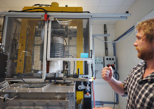
Figure 1. Francois Chancerel presenting an inductive heating hot press specially designed by S’Tile for silicon sintering. It can produce up to 235 mm round sintered wafers.
Designing an Inexpensive, Highly Efficient Solar Cell
The application of solar cell technology depends on cost vs. energy efficiency (i.e., the amount of light transformed into electricity). The i-Cell solar cell design, illustrated in Figure 2 below, minimizes this ratio in several ways:
- The photon-harvesting layer is made of an ultra-thin layer of p-type monocrystalline silicon (MonoSi).
- An inexpensive silicon supporting solar-grade layer protects against breakages, reducing costs compared to conventional solar cells with thick solar-grade silicon layers.
- Reduced size of metallic contacts cuts silver use by 50% and copper by 90%.
- Four subcells connected in series reduce the current and increase the voltage through electrodes. This improves energy efficiency due to a decrease in resistive losses during module integration. Commercially viable efficiencies of over 18% have been accomplished with the i-Cell.
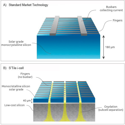
Figure 2. The S’Tile i-Cell solar cell design. A) Conventional designs use a thick layer of expensive MonoSi, with thick metallic contacts. B) The i-Cell supports ultra-thin p-type MonoSi with low-cost sintered silicon, with a connective wafer. Sub-cells interconnected in series with finger-shaped contacts reduces resistive current loss.
Optimizing the Fabrication Process of the i-Cell Solar Cell
The fabrication process of the i-Cell commands the cost-performance ratio, and this includes a number of steps, as outlined in the following:
1. Substrate Fabrication
The substrate is formed by sintering low-grade silicon powder. When heat and pressure are applied, sintering produces a dense layer from a powder. This process is highly dependent on grain size and the silicon powder’s morphology.
S’Tile previously used laser granulometry to determine the grain size and distribution. While this technique is fast, it does not provide information on grain morphology. So S’Tile turned to digital microscopy, a complementary technique that can visualize the grain geometry for efficient inspections (Figure 3).
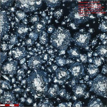
Figure 3. Silicon powder inspection guides sintering conditions. Size and shape of grains can be inspected with the automatic software of the Evident DSX500.
We used the granulometry software. Evident helped us in correcting our sample preparation protocol, and with the sample analysis software to separate grain boundaries.
Francois Chancerel, Engineer, S’Tile
2. Inspecting the Conductive Wells in the Substrate
Conductive wells are etched in the silicon substrate to connect the substrate, overlying connective wafer, and MonoSi (Figure 2). Well shape and depth impact current transport inside the sintered substrate.
Francois explained, “If we change the process, we need to know how this alters the wells. Do we have a consistent depth? With the DSX500, it was really easy to see this using the layer thickness measurement tool [Figure 4].”
Electrical connectivity, the primary property of these wells, can be measured through electrical resistance. It is also critical to understand how well shape and depth interact with the substrate and if they damage the surface. The DSX500 digital microscope detects these properties, complementing the primary measurement tool.
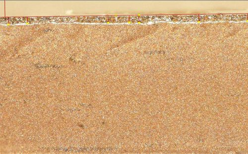
Figure 4. Measuring thickness of conductive wells. Layer measuring microscope for this purpose. Thickness measurement software of the DSX500 was employed, as visualized with polarized imaging.
3. Layering
The two silicon layers are bonded using a proprietary process.
Francois explained, “It is crucial to have a perfect surface on the MonoSi, as any breaks compromise the electrical capability of the layer.”
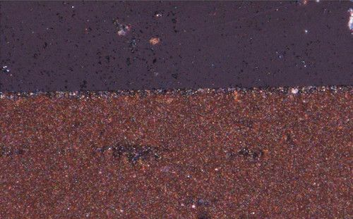
Figure 5. Inspecting the bonding between silicon layers. Bonding quality was analyzed with polarized imaging chosen from the Best Image Function of the DSX500. At 4,000x magnification, it can be verified that the MonoSi remains undamaged, with perfect contact and no voids at the interface.
In a conventional inspection of the bonding quality between layers, samples are cut as cross-sections and analyzed for any breaks or voids. In contrast, the DSX500 digital microscope requires less sample preparation due to the high dynamic range digital tool that generates a fully-focused image from different Z-layers.
“With the DSX500, we can generate high-quality images from the first shot with every feature in focus,” said Francois.
The ability to avoid sample polishing is another notable benefit.
Francois explained, “With 2D microscopy, we need to polish the sample, which is time consuming and can also damage the silicon wafer. It is then impossible to know if the breaks were due to the fabrication process or sample preparation.”
4. Measuring Surface Texturization to Reduce Reflection
When light hits a flat silicon surface, about 30% is reflected instead of absorbed. Minimizing reflectivity is crucial for solar cells, and it can be achieved in two ways: an additional anti-reflective layer and surface texturization.
3D confocal laser scanning microscopes are ideal for measuring surface texture due to their high-resolution imaging capabilities. S’Tile used the LEXT OLS4100 3D laser confocal microscope to measure the surface texture.
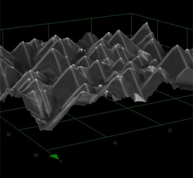
Figure 6. Measuring surface texture to reduce reflection. High-resolution characterization is achieved through the antireflective coating using the LEXT OLS4100 3D confocal laser scanning microscope. The detailed surface texture information enables S’Tile to assess the texturization process and reduce light reflection.
The pyramid morphology of the surface (Figure 6) reduces reflection, capturing and constantly re-reflecting light between each pyramid. Shape, distribution, and height are important properties that can be optimized through fabrication.
However, S’Tile realized that the limited resolution of a conventional microscope makes it difficult to measure the height differences.
We tested different protocols and compared the success of each based on surface texture using standard widefield light microscopy. However, with the height differences being in some cases just one micron, the limited resolution meant this was not possible.
Mr. Francois Chancerel, Engineer, S’Tile
They found the LEXT confocal laser microscope provided the image quality they needed to perform this task.
Francois explained, “Achieving this quality of images with a light microscope is new to us, and they are comparable to electron microscopy. We found it impressive to use the LEXT.”
Combining an optimized surface texture with an anti-reflection layer makes it possible to reduce reflection to 5% or 10% for improved energy efficiency.
5. Engraving
To form the network of electrodes overlaying the MonoSi surface, laser scribing creates channels in the silicon to be filled with silver.
When inspecting the engraving process, it is critical to gather information on a range of properties. Well depth and shape determine electrode morphology, and therefore resistance. Laser scribing can control a variety of parameters, such as intensity and wavelengths, to adjust the width and depth.
Previously, with the 2D microscope, we were unable to produce 3D images, and although we could inspect the depth of the wells, we could not perform this completely along the wells for a complete picture, like we now can with the DSX500 [Figure 7].
Mr. Francois Chancerel, Engineer, S’Tile
It is also important to inspect surface integrity, since a smooth surface is needed to fabricate the interconnections between subcells. Inspectors also need to know if the laser is damaging the silicon because the laser parameters can be modulated for the smoothest surface. Users can see damaged surfaces quickly and easily with the DSX500 digital microscope.
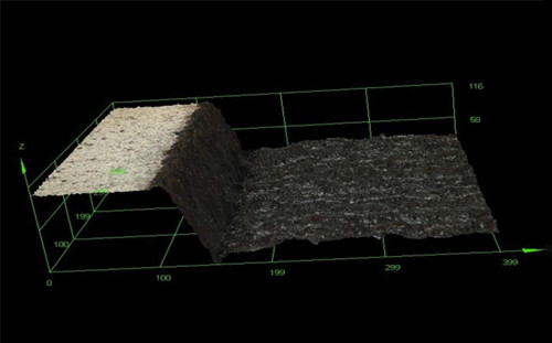
Figure 7. Well shape and surface integrity inspected after laser engraving. High-resolution 3D imaging with the DSX500 enables inspection of well morphology and surface integrity, optimizing laser engraving parameters and avoiding surface damage.
6. Metallization & Firing
The metallization process of adding silver into the engraved channels is performed using screen printing, and the form of the electrodes has a substantial impact on solar cell efficiency.
Francois explained, “A larger surface area minimizes resistive losses, but a really thin strip maximizes the surface area of the photon-harvesting silicon.”
Screen printing has many parameters to control, so S’Tile used the Evident DSX500 digital microscope to capture and analyze 3D images of the silver electrodes (Figure 8) and get a better understanding of their properties.
“The height mapping function is highly accurate, providing a comprehensive view instead of individual points.” Francois said about the DSX500 microscope, “We can measure volume, average surface area, and minimum surface area, enabling us to judge the quality of a metallization protocol.”
He added, “The DSX has really helped advance our metallization process. We previously had to analyze cross-sections, and so were limited to testing final samples, only finding the best printing and firing combination. With 3D analysis of printed samples, we can separate the steps and easily optimize each step individually.”
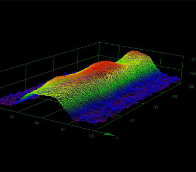
Figure 8. Inspecting electrode grid morphology. Height and width of the finger grid can be modulated from screen printing optimization to minimize resistive and optical losses. Inspecting the metallization helps guide this process, using the DSX500 3D analysis software at 100x magnification.
Summary
The Evident DSX series digital microscope and LEXT series laser confocal microscope, combined with other specialized methods, enable efficient inspections for every part of the i-Cell solar cell manufacturing process.
Francois remarked, “We can now understand much more clearly why one protocol leads to better results, and our different measurement tools fit together to guide the complete process optimization.”

This information has been sourced, reviewed and adapted from materials provided by Evident Corporation - Industrial Microscopy.
For more information on this source, please visit Evident Corporation - Industrial Microscopy