Sponsored by MerckJan 4 2021
Lithography, based on conventional ink-printing processes, is a technique for patterning a variety of layers, such as conductors, semiconductors, or dielectrics, on a surface. Nanopatterning stretches traditional lithographic techniques into the submicron scale.
Therefore, your materials needs for lithography and nanopatterning are within reach utilizing complete line of monomers, polymers, inks, resins, silanes, surfactants and other related products. The company offers resist materials, polyelectrolytes for self-assembled monolayers (SAMS), photoacid generators (PAGs), fluorine-containing monomers for 157 nm UV resists and high-purity norbornadiene. Research and bulk quantities of all materials are also available.
Lithography
A standard integrated circuit is comprised of numerous patterned thin films of metals, dielectrics and semiconductors on a variety of substrates such as silicon, germanium or gallium arsenide. Such a device is manufactured using a technology known as lithography, in which radiation sensitive polymeric materials known as resists are utilized to generate circuit patterns in the substrates. Figure 1 exhibits the conventional sequence of the lithographic process.
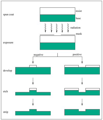
Figure 1. Schematic representation of the lithographic process.1 Image Credit: Merck
Application of the resist material is performed, usually by spin coating over the substrate (wafer) as a thin coating and then heated to withdraw the casting solvent (post-apply bake, pre-exposure bake, or pre-bake). The resist film is then exposed in an image-wise fashion via a mask (in photo- and X-ray lithography) or first-hand with acutely focused electron beams.
The resist film that is exposed is subsequently developed, generally by immersion in a developer solvent to produce three-dimensional relief images. The exposure may make the resist film more soluble in the developer, consequently generating a positive-tone image of the mask.
In contrast, it may be rendered less soluble upon exposure, leading to the generation of a negative-tone image. When transference of the resist image into the substrate by etching and related techniques is completed, the resist film that is left behind after the development acts as a protective mask. The resist film must ‘resist’ the etchant and shield the underlying substrate while the areas that are bared are being etched.
The last of the resist film is eventually stripped, leaving an image of the preferred circuit in the substrate. The process is repeated over and over to manufacture complex semiconductor devices.1
For a resist material to be useful in device fabrication:
- it must be capable of spin casting from solution into a thin and uniform film that adheres to various substrates such as metals, semiconductors and insulators
- withstand extremely harsh environments, for example, high temperature, strong corrosive acids and plasmas such as used in subsequent etching, doping and sputtering operations.
- possess high resolution capability, dictated by solubility/insolubility characteristics
- possess high radiation sensitivity
In previous generations of resists (often predicated on novolok phenolformaldehyde polymers), each absorbed quantum of radiation created – on average – less than one chemical reaction inside the material. As early as 1973, Smith described ‘Photosolubilizable compositions’ for photographic and photoresist applications with overall quantum yields exceeding one.2 While the concept was limited in practice, thermostable yet photosensitive onium salts of strong acids developed by Crivello as PAGs for cationic photopolymerization presented new opportunities.3
The university industry team of Fréchet (University of Ottawa) and Wilson and Ito (IBM Inc.) noted the first CA resist for microlithography.4 The team combined onium salts with the acid-deprotectable poly(4-[t-butyloxycarbonyloxy]styrene) (poly-TBOCST) and coined the term chemical amplification. Between January 1992 and June 1994, more than 200 articles and numerous reviews have materialized on this topic alone.5-10
In chemical amplification (CA) resists, the principal photochemical event generates a mobile catalyst that, commonly during subsequent postexposure baking (PEB), goes on to cause a torrent of secondary catalytic events within a 5-25 nm radius that transform the material. Such chemical amplification enables an overall quantum yield (the amount of material reactions divided by number of absorbed photons) of up to several hundred. Therefore, a CA resist must be composed of:
- a limited amount (ca. 1-5 wt%) of radiation-sensitive catalyst precursor, typically a photoacid generator (PAG);
- several chemical groups that can react by addition, elimination, or rearrangement only in the presence of catalyst;
- polymer matrix able to scatter all other components in a smooth clear film; and
- optional additives to enhance processability or performance; e.g., surfactants, photosensitizers and etch resistors.
While the catalyst-sensitive groups are polymer-bound and the catalyst precursors are free in most reported compositions (i.e., i + ii~iii), components i-iii or iv can in theory be interlinked in any combination, as small molecules, copolymers, homopolymers, or blends (e.g., i + ii + iii, i~ii + iii, i~ii~iii).1-4
Along with their greater sensitivity and contrast in producing images, CA are also better than previous resists when it comes to being more flexible in design and formulation. They are also more versatile in radiation source (electromagnetic or particle beams) and compatible with dry (plasma), multilayer and other state-of-the-art pattern transfer techniques.
Resist systems can generally be classified in accordance with their design, namely, one-, two-, or multi-component systems. One-component resist systems are made up of pure polymers that should united all the necessary attributes such as radiation sensitivity, substrate protection and film-forming characteristics. The most sought after resist designs in contemporary lithography are predicated on two-component systems in which resist functions are supplied by two separate components.
On the basis of the radiation source, it is possible to separate resist systems into three groups: UV or photoresists, electron-beam resists and X-ray resists. Photolithography that uses UV light has been the principal technology in semiconductor fabrication and will likely continue to be so in the foreseeable future. X-ray lithography has the capacity to produce high-resolution, high-aspect-ratio (height-width) images and is regarded the technology of the future, whereas electron-beam lithography is often utilized in photomask fabrication.
Photolithography can be subdivided further into near-UV (350-450 nm), mid-UV (300-350 nm) and deep-UV (<300 nm) technologies, based on the wavelength of the exposure. While the resolution corresponds to the exposing wavelength it is inversely proportional to the numerical aperture (NA) of the lens. Therefore, the i-line (365 nm) with a high-NA lens shifting from the g-line (436 nm), is considered to be the principal technology in the manufacture of 16-megabit (Mbit) dynamic random access memory (DRAM) devices with a minimum feature size of 0.5 mm.
It transpires that krypton fluoride (KrF, 248 nm), argon fluoride (ArF, 193 nm) and F2 (157 nm) excimer laser technologies are developing, while the minimum feature size continues to decreased to numbers below 0.5 mm an down to 80 nm.11
The quantum leap that eventually led to the adoption of 248 nm lithography as the technology of choice for progressive device manufacture was the advancement of CA resists. Photolithography using 193 nm light has become the consensus candidate for the next-generation of optical lithography tools. At this wavelength, the opacity of conventional aromatic-based materials prevents their use.
Investigation of alternative resist materials predicated on aliphatic polymers and dissolution inhibitors has been conducted.10 The inception of monomers bearing cyclic side groups such as adamantyl or norbornyl considerably enhances the etch resistance over that of simple acrylic polymers. Conversely, alicyclic structures have been directly included into the polymer backbone providing a second route to 193 nm single layer resists.12
The next-generation of optical lithography at 157 nm has demanded new developments in resist technology. Single-layer 248 nm and 193 nm photoresists are not an appropriate substitute due to their high optical absorbance at 157 nm. The inclusion of fluorine into polymers has opened the door to suitable resist materials.13
Nanoimprint Lithography
Imprinting, or embossing, is a common technique regarding the generation of microstructures in hard polymers by compressing a rigid master comprised of surface-relief features into a thin thermoplastic polymer film that is subsequently heated close to or, more typically, above the Tg (see Figure 2).14
Nanoimprint lithography (NIL) has the possibility of high-throughput because of the parallel processing, does not necessitate sophisticated tools and enables nanoscale replication for data storage.15,16 NIL is also compatible with traditional device processing methods. There are a number of experimental parameters like T, viscosity in the melt, adhesion of the polymer to the mold, etc. that determine the quality of the nanoimprinting process.17
PMMA has found its general use as the material that can be printed on, but a range of thermoplastic and thermosetting polymers is being researched to improve imprinting and subsequent etching steps.18,19
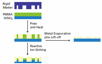
Figure 2. Schematic overview of nanoimprint lithography. Image Credit: Merck
The rigid master is typically prepared via e-beam lithography and has feature sizes in the 10–100 nm size range. Once imprinting of the polymer film has been carried out additional etching can move the pattern into the underlying substrate. Metal evaporation and lift-off of the polymer mask further generates nano scaled patterned metal features.
Soft Lithography
Nanoimprint lithography (NIL) has typically been used to emboss hard thermoplastic polymers. The micromolding and embossing of elastomers has garnered significant interest as these materials have become integral to applications in softlitho graphic techniques such as microcontact printing (mCP).20,21 This technique involves a monolayer of a material being printed off an elastomeric stamp [made of poly(dimethylsiloxane) (PDMS)] after establishing conformal contact between stamp and substrate (Figure 3).
Sub-micron surface relief structures can be introduced easily in PDMS by curing the polymers against a lithographically prepared master. The benefits of mCP is that it allows for the surfaces to be patterned chemically at the sub-micron level.
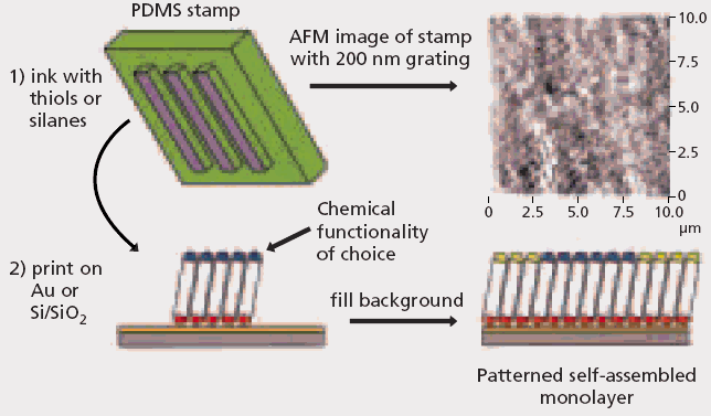
Figure 3. Schematic overview of microcontact printing (mCP). (Images courtesy of Hongwei Li, Wilhelm T. S. Huck; University of Cambridge , Department of Chemistry, Melville Laboratory for Polymer Synthesis.)
An elastomeric stamp is connected to small molecules (thiols or silanes) and stamped against a clean substrate (gold or silicon wafer). Where the stamp comes into contact with the surface, a monolayer of material is passed on to the substrate. To fill in the background, a second thiol or silane is used to generate a chemically patterned surface.
Photochemical Acid Generators
Photoacid generators (or PAGs) are cationic photoinitiators. A photoinitiator is a compound specifically added to a formulation to transform absorbed light energy, UV or visible light, into chemical energy in the form of initiating species, viz., free radicals or cations.
Cationic photoinitiators are broadly utilized in optical lithography. The capacity of various types of cationic photoinitiators to act as dormant photochemical sources of robust protonic or Lewis acids is the reason for their use in photoimaging applications. The continuous decrease in the dimensions of devices in the microelectronics industry is coming about by pushing the limits of optical lithography. In chemically amplified resist technology, the radiation-sensitive material (resist) in which patterns are characterized is generally comprised of a matrix polymer and an onium salt photoacid generator (or PAG).10
There are numerous materials’ issues to be taken into account when selecting the PAG: appropriate radiation sensitivity to guarantee appropriate acid generation for good resist sensitivity, non-presence of metallic elements, temperature stability, etc.22
Strong acid is typically considered to be the photo-supplied catalyst as standard. Triarylsulfonium and diaryliodonium salts have become the conventional PAG ingredients in CA resist formulations. This is due to their basic properties which includes easy synthesis, high quantum yield for acid (and also radical) generation, thermal stability and the strength and nonvolatility of the acids they supply.23
Uncomplicated onium salts possess a direct sensitivity to DUV, X-ray and electron radiations and can therefore be structurally adapted, or blended with photosensitizers, to also work well at mid-UV and longer wavelengths. Yet, onium salts are ionic and most will phase separate from some apolar polymers, or not completely dissolve in some of the casting solvents. Nonionic PAGs such as phloroglucinyl and o,o-dinitrobenzyl sulfonates, benzylsulfones and some 1,1,1-trihalides are better suited when generally using hydrophobic media, although their quantum yields for acid generation and thermal stabilities are often lower.24
Advances in optical lithography are in part responsible for the extraordinary rate of increase in the integration density of silicon chips – the process, as previously outlined, patterns and guides the manufacture of the component semiconductor circuitry and devices. Although the development of resolution enhancement techniques and shorter-wavelength light sources should sustain the current rate of device miniaturization for a few more years, the will come a point in time when optical lithography is not able to achieve the necessary feature sizes.25
Multiple alternative lithographic methods are being developed and they demonstrate the capacity to overcome these resolution limits – EUV, X-ray, electron beam and ion beam lithographies, but, as it stands no clear successor to optical lithography has come forward.
Nanopatterning
Fabrication methods for sub-micron length scales are spread across a wide range, from state-of-the-art lithographic methods that have their basis in the semiconductor industry to more current materials and advances in chemistry that depend on self-organization. For characterizing patterns below 100 nm, there are multiple approaches that have been suggested (and indeed demonstrated). These include near-field optical lithography, direct patterning on a nanometer scale with scanning-probe microscopes, nano-imprint lithography (including micro-contact printing, mold-assisted lithography and hot embossing lithography), pattern formation based on phase separation of polymers, self-assembly of monolayers, etc.
The search goes on for nonphotolithographic techniques that could offer cost-effective and simple technological nanofabrication strategies. Some of these propositions are more appropriate for generating individual nano-structures for the study of nanometer-scale devices; the low throughput always likely to remain impracticable for commercial application. Others, including nanoimprint lithography, offer the potential of high throughput due to parallel processing and they do not necessitate sophisticated tools, while enabling nanoscale replication for data storage.15,16
Their morphologies in the bulk and natural length scales of polymer chains, which lie in the nanometer domain, make polymers the perfect building blocks for nanopatterning. Recent progress in the use of polymers for the manufacturing of nanostructures via lithographic and self-assembling strategies has been reviewed.26
Nanopatterning via Phase Separation of Polymers
Block copolymers of flexible, chemically incompatible and dissimilar blocks can microphase separate into a range of different morphologies with nanometer scale dimensions. This self-assembly process is guided by an opposing mixing enthalpy and a small mixing entropy, while the covalent bond between the two blocks inhibits macrophase separation. When the microphase separated morphology can be manipulated and transformed into a useful structure, phase separation of block copolymers can be an influential tool for the manufacture of nanostructures without adding lithography and processing steps.27
To prevent copolymers copolymers, random copolymers made up of components suitably dissimilar predicated on size and chemical nature, for e.g., SSQ/Polypropylene blend, SSQ-MMA copolymer, or physical blends of hydrophobic and hydrophilic polymers guided by an fundamental pattern of incompatibility have been shown to generate arbitrary yet functional patterns.26,28 The use of surfactants in such blends may be utilized to highlight the various areas of surface tension.
Soft lithographic approaches have been used in combination with surfactant and particulate templating strategies to generate hierarchically ordered oxides.29 A recent report unites macroscopic, evaporative printing procedures and molecular scale, evaporation-induced self-assembly (EISA) of organically modified mesophases. This enables the accelerated fabrication of hierarchical structures displaying form and function across several length scales and at multiple locations. The formulation of the ‘ink’ in such hierarchical assembly strategies is complicated and may require a wide-variety of surfactants.30
Self-Assembled Monolayer Systems (SAMS)
Polyelectrolytes are identified as materials for which electrostatic interactions over distances larger than typical molecular dimensions govern the solution properties in solvents of high dielectric constant.1,31 These materials are predominately used in industrial applications as dispersants in aqueous media, for sizing in textile and paper manufacture, flocculating agents to coagulate slurries and industrial wastes and as conditioning additives to drilling muds and soil to shield against abrasive damage. In recent times, they have been put into service for molecular self-assembly methods for thin film deposition of electrically conducting polymers,32 nanoparticles,33 conjugated polymers for light emitting devices,34 and non-centrosymmetric-ordered second order nonlinear optical (NLO) devices.35
The technique of Self-Assembled Monolayers or SAMs is a creative and straightforward, yet powerful nanoscale approach for the manufacture of practical supramolecular assemblies for numerous device applications.36-40 It requires the alternate adsorption of anionic and cationic polyelectrolytes onto a suitable substrate.
Only one of these is generally the active layer, while the other facilitates the binding of the composite multilayered film by electrostatic attraction. Conversely, the oppositely charged polyelectrolytes may act as a barrier for the perpetual release of an active core. Well-managed formation of exceptionally ordered, multifunctional, three-dimensional, reactive, thin films containing biological molecules is witnessing extensive application in the areas of biotechnology and biomaterials science.41,42
Of the possible polyanionic candidates, poly(styrenesulfonic acid) (PSSA) and its salts have been utilized to a great extent.40 Why? Superb adsorption properties, smooth films with easily controllable thickness, water solubility, controlled level of loading/penetration of active component—all properties crucial in the realization of high performance devices predicated on supramolecular structures in terms of sensitivity, selectivity, stability and response time. Additionally, PSSA has been used to dope thiophene-based conjugated polymers to make them conducting, e.g., PEDOT/PSS (Product Nos. 483095 and 560596). Post-treatment of polyaniline (emeraldine salt), grafted to lignin (see Product Nos. 561096; 561118; 561126; 561134), with PSSA may also be used to improved electrical conductivity.
Norbornadiene
A quick survey of the scientific and patent literature identifies that this dynamic monomer has been applied over a wide-range of high technology applications, in fields ranging from pharmaceutical, materials science and ag-related, to being used as a model system in basic research activity (for example, in testing new nanocatalysts - in single-step hydrogenations,43,44 tandem cycloaddition reactions,45 Pauson-Khand annelation46,47 as well as in detailed theoretical studies.48,49 The novel set of properties provided by Norbornadiene along with its modifications driving some of the reported applications are exhibited in the following table.
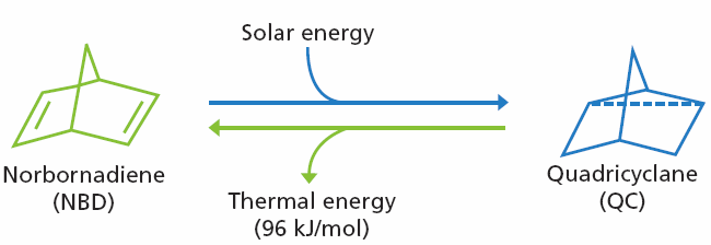
Scheme 1. Conversion between norbornadiene (NBD) and quadricylane (QC). Image Credit: Merck
Table 1. Properties of norbornadiene. Source: Merck
| NBD Property |
Transformation |
Application of NBD |
| Bicyclic, strained system |
Undergoes photochemical valence isomerization to Quadricyclane (QC), converting solar energy to strain energy
(See Scheme 1) |
Solar energy storage system8 |
| Bicyclic, strained system |
Strain energy released gradually as heat upon conversion back to NBD
(See Scheme 1) |
Microheater9; Energetic binder for solid rocket propellants10 |
| Diolefin |
Starter for norbornenediol derivative to synthesize stereo-controlled ROMP-derived precursor polymer, which upon thermal elimination results in a special form of polyacetylene |
Synthon for Conductive Polymer, polyacetylene11,12 |
| Cycloaliphatic Monomer |
Controlled cyclopolymerization of bulky ester derivatives of NBD to afford regioregular 2-alkoxycarbonyl nortricyclene polymers |
New resist materials based on cycloaliphatic polymers for imaging with 193 nm lasers13 |
| Rigid, 3-D, crosslinking agent |
Synthesis of soybean oilstyrene-NBD thermosetting copolymers |
Shape memory polymer with Tg well above ambient14 |
| NBD |
ROMP synthesized fluoropolymer, poly[2,3-bis (trifluoromethyl)NBD] having usefully high values of pyroelectric properties combined with low dielectric loss at RT |
Pyroelectric transducer with a figure of merit comparable or better than that of PVDF15 |
| NBD |
Controlled selectivity and reaction rate for cyclic dimerization, co-dimerization, isomerization and allylation of NBD |
As a universal substrate for organic and petrochemical synthesis of wide range of rare polycyclic hydrocarbons16 |
| NBD |
Inhibited ethylene production and RNAase induction in apple pulp tissue |
Growth regulator in fruit production17 |
| Highly strained NBD |
Reagent in the Pd-catalyzed conversion of hydrosilanes to alkoxysilanes |
Efficient hydrogen scavenger18 |
| Bicyclic NB |
Starter in a fifteen step synthesis of (+)-Sparteine |
Synthon in the first asymmetric total synthesis of (+)-Sparteine19 |
References and Further Reading
- Specialty Polymers; Dyson, R.W., Ed.; Chapman and Hall: New York, NY 1987; p 110 (Catalog No. Z22,414-6).
- Smith, G. H.; Bonham, J. A. U.S. Patent 3 779 778, 1973.
- Crivello, J. V.; Lam, J. H. W. J. Polym. Sci. 1976, 56, 389.
- Frechet, J. M. J.; Eichler, E.; Willson, C. G.; Ito, H. Polymer 1983, 24, 995.
- Reichmanis, E.; Houlihan, F. M.; Nalamasu, O.; Neenan, T. X. In Polymers for Microelectronics; American Chemical Society: Washington, DC, USA, ACS Symp. Ser. 537, 1994.
- MacDonald, S. A.; Willson, C. G.; Frechet, J. M. J. Acc. Chem. Res. 1994, 27, 151.
- Ito, H. Jpn. J. Appl. Phys., Part 1 1992, 31, 4273.
- Frechet, J. M. J. et al. J. Photopolym. Sci. Technol. 1992, 5, 17.
- Burggraff, P. Semiconductor International 1994, 17, 56.
- Walraff, G.M.; Hinsberg, W.D. Chem Rev. 1999, 99, 1801.
- Service, R.F. Science 2001, 293.
- Meagley, R.P. et al. Chem. Comm. 1999, 1587.
- Brodsky, et al. J. Va. Sci. Technol. B 2000, 18, 3396.
- Herzig, E.P. Micro-optics, London: Taylor & Francis, 1997.
- Terris, B.D. et al. Appl. Phys. Lett. 1996, 69, 4262.
- Li, M. et al. Appl. Phys. Lett. 2000, 76, 673.
- Faircloth, B. et al. J. Vac. Sci. Technol. B 2000, 18,1866.
- Schulz, H. et al. J. Vac. Sci. Technol.B 2000, 18,1861.
- Schulz, H. et al. J. Vac. Sci. Technol. B 2000, 18, 3582.
- Xia, Y. Angew. Chem. Int. Ed. 1998, 37, 550.
- Michel, B. et al. IBM J. Res. Dev. 2001, 45, 697.
- Reichmanis, E. et al. ibid. 1991, 3, 394.
- Crivello, J.V. "Initiators of Polyreactions-Polyactivity"; Springer-Verlag: berlin, Advances in Polymer Science, 62, 1, 1982.
- Houlihan, F.M; et al. In Polymers for Microelectornics; American Chemical Society: Washington, DC, USA, ACS Symp. Ser. 537, 1994, 25.
- Ito, T.; Okazaki, S. Nature 2000, 406, 1027.
- Hongwei, L.; Wilhelm, T.S.H. Current Opinion in Solid State and Materials Science 2002, 6, 3.
- Klok, H.A.; Lecommandoux, S. Adv. Mater. 2001, 13, 1217.
- Schwab, J. et al. Polymer Preprints 2001, 42, 48.
- Yang, P. et al. Science 1998, 282, 2244.
- Fan, H. et al. Nature 2000, 405, 56.
- For a discussion of the differences between polyelectrolytes and ionomers, see: Eisenberg, A.; Kim, J-S. Introduction to Ionomers; John Wiley: New York, NY 1998 (Catalog No. Z41,033-0).
- Sayre, C.N.; Collard, D.M. J. Mater. Chem. 1997, 7, 909.
- Schmitt, J. et al. Adv. Mater. 1997, 9, 61.
- Cheung, J. et al. Polym. Prepr. 1993, 34, 757.
- Wang, X. et al. Macromol. Rapid Commun. 1997, 18, 451.
- Tedeschi, C. et al. J. Am. Chem. Soc. 2001, 123, 954.
- Lee, S.-H. et al. Langmuir 2000, 16, 10482.
- Stair, J.L. et al. Chem. Mater. 2001, 13, 2641.
- Suzuki, I. et al. Macromolecules 2002, 35, 577.
- For a comprehensive list of literature references from 1966 through June 2001, see Polyelectrolyte Multilayers Home Page.
- Santos, J.P. et al. Langmuir 2001, 17, 5361.
- Strohoff, J.J.; Mirkin, C.A. Chem. Rev. 1999, 99, 1849.
- Thomas, J.M. et al. Acc. Chem. Res. 2003, 36, 20.
- Raja, R; Thomas, J.M. Studies in Surf. Sci. and Catalysis 2002, 141 (Nanoporous Materials III), 317.
- Barluenga, J. et al. J. Am. Chem. Soc. 2002, 124, 10978.
- Son, S.U. et al. Org. Lett. 2002, 4, 3983.
- Gibson, S.E. et al. Tetrahedron 2002, 58, 4937.
- Mackenzie-Ross, H. et al. J. Phys. Chem. A 2002, 106, 9573.
- Kishimoto, N. et al. Bull. Chem. Soc. Jap. 2002, 75, 1503.
- Nishikubo, T., et al. Macromolecules 1992, 25, 4469.
- Morino, S. et al. J. Photopolym. Sci. Technol. 1994, 7, 121.
- Wright, M.E.; Allred, G.D. J. Org. Chem. 1993, 58, 4122.
- Stelzer, F. Lecture at the 8th Symposium on Olefin Metathesis, Bayreuth (Germany), 4-9. September, 1989.
- Bazan, G. C. et al. Macromolecules 1991, 24, 4495.
- Niu, J. et al. Angew. Chem. 1998, 110, 685.
- Li, F.; Larock, R.C. J. Appl. Poly. Sci. 2002, 84, 1533.
- Davies, G.R. et al. Polymer 1995, 36, 235.
- Flid, V.R. et al. Eurasian Chemico-Technological J. 2001, 3, 73.
- Treccani, C.P. et al. ISHS Acta Horticulturae 179: V International symposium.
- Sudhakar, S.; Luh, T.-Y. J. Org. Chem. 2002, 67, 6860.
- Smith, B.T. et al. Org Lett. 2002, 4, 2577.

This information has been sourced, reviewed and adapted from materials provided by Merck.
For more information on this source, please visit Merck.