In the coming years, the production of silicon wafers is expected to grow thanks to increased demand for semiconductors. This is especially true in the industries of consumer electronics and automotive, as well as the use of silicon devices in the booming solar power industry.
In order to produce silicon wafers, a range of different manufacturing methods is used.
The two most common of these are the Zone (FZ) and Czochralski (CZ) processes, respectively. The former process - the FZ process - yields high purity silicon wafers, while the latter process - the CZ process – creates wafers with elemental impurities, in particular carbon and oxygen.
It must be said, however, that the CZ process holds some key advantages over the FZ process, including things like faster manufacturing, a lower cost, and the thermal stress properties of the wafer itself.
The presence of oxygen impurities can also have a positive benefit as it then removes trace metal impurities, acting as a getter. This helps to explain why the CZ process is the most widely adopted in the industry when it comes to silicon wafer manufacturing.
It is important to determine the levels of carbon and oxygen impurities in silicon wafers in order to ensure they are not too high - which can lead to electrically active defects and product failure/rejection. Rapid and easy measurement is offered by infrared to determine impurity levels according to global standard methods.1,2,3,4
Methods and Materials
The measurement system is comprised of a PerkinElmer Spectrum 3™ FT-IR spectrometer, which has a MappIR wafer holder and optical system with automation software, as depicted by Figure 1.
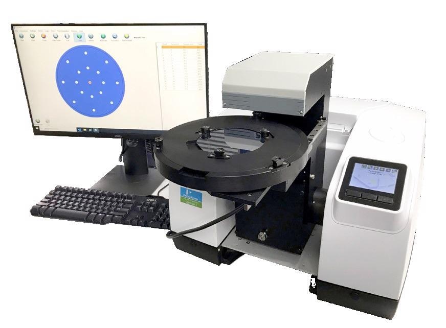
Figure 1. The Spectrum 3 FT-IR and MappIR System. Image Credit: PerkinElmer, Inc.
A range of wafer sizes, from 2 inches up to 8 inches (MappIR) or 12 inches (Mapp300), can be analyzed by the system in either transmission or reflection mode.
Automated, unattended mapping of the wafer is facilitated by the automation software, collecting spectra from the width of the entire wafer in accordance with pre-set or user-defined mapping arrangements. Calculations follow the data collection, according to the analysis method specified.
Transmission mode was used to collect spectra for a range of 6-inch diameter silicon wafers at a spectral resolution of 4 cm-1 using 32 scans for data collection. Dry nitrogen was used to continuously purge the Spectrum 3 and MappIR in order to remove atmospheric spectral interferences from the spectra.
Figure 2 shows a spectrum of a 500 microns thick Float Zone silicon wafer.
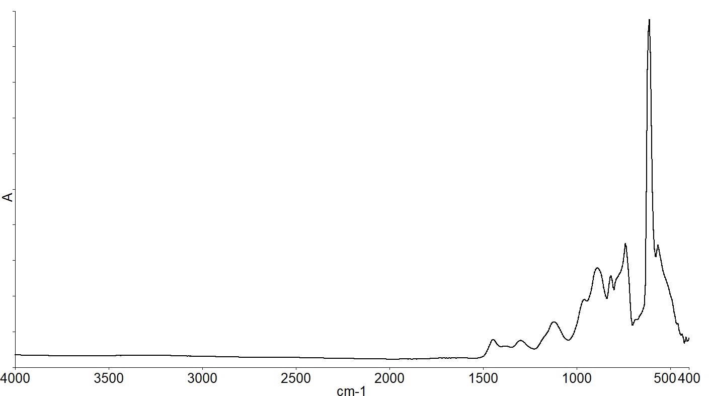
Figure 2. The infrared spectrum of a Float Zone silicon wafer. Image Credit: PerkinElmer, Inc.
There are several absorption bands below 1500 cm-1 due to the silicon lattice vibrations, as shown by the infrared spectrum. Spectra of the same FZ wafer and a CZ wafer overlaid zooming in on the spectral range below 1500 cm-1 are shown in Figure 3.
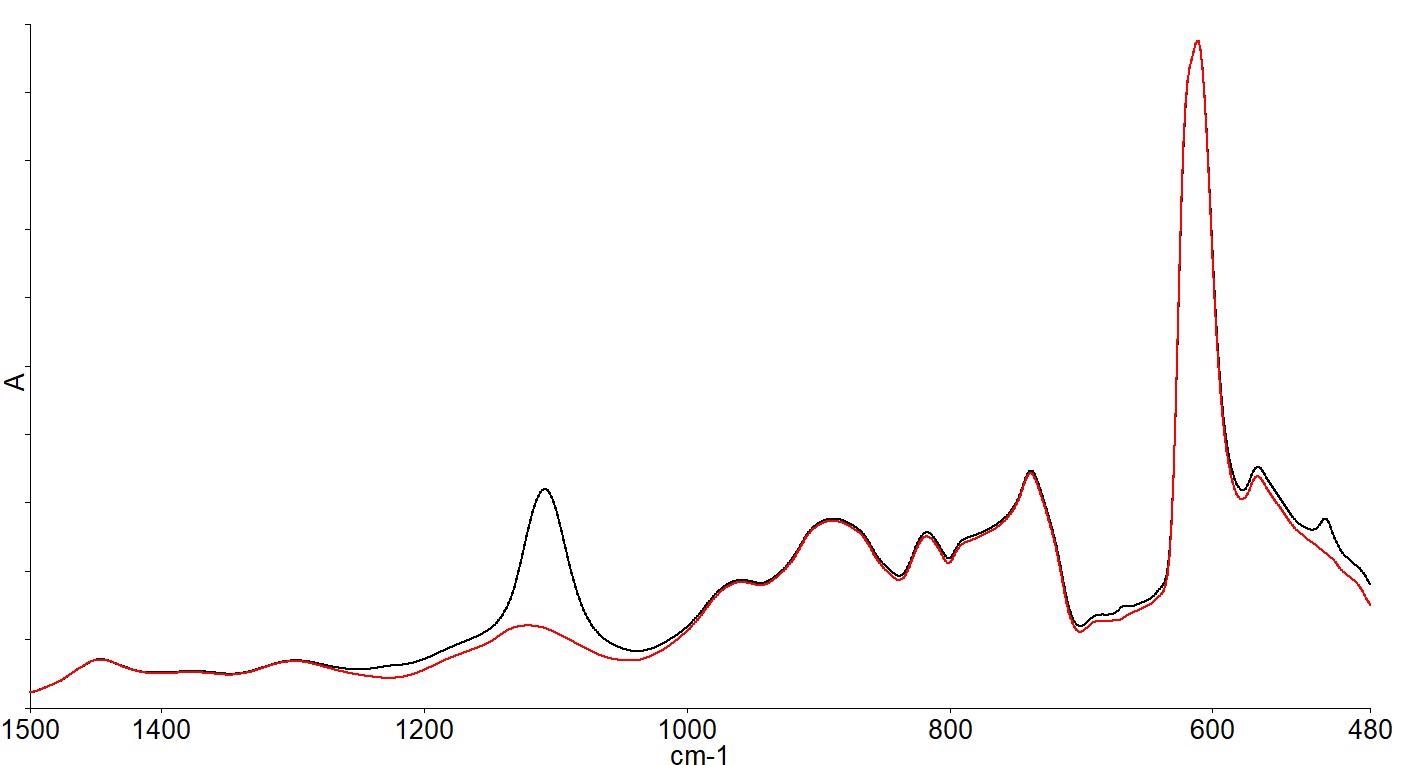
Figure 3. FZ wafer spectrum (red) and CZ wafer spectrum (black) showing spectral differences. Image Credit: PerkinElmer, Inc.
The spectra show that there are differences between the two wafer spectra; in particular, the additional band around 1100 cm-1 in the CZ spectrum.
The standard methods specify the subtraction of the high purity FZ reference wafer spectrum from the CZ sample being analyzed in order to see the spectral differences more clearly and to perform calculations on the spectra. This generates a spectrum (as depicted by Figure 4).
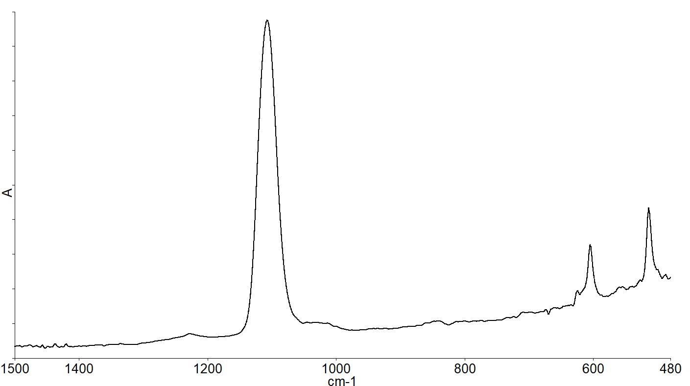
Figure 4. Subtraction spectrum of CZ-FZ wafer spectra showing bands due to impurities in the CZ material. Image Credit: PerkinElmer, Inc.
The interstitial oxygen present causes the bands at 1107 and 513 cm-1, while the substitutional carbon present causes the band at 605 cm-1. Quantitative analysis can then be performed on the spectra. Figure 5 depicts the spectra of wafers with a range of different oxygen concentrations.
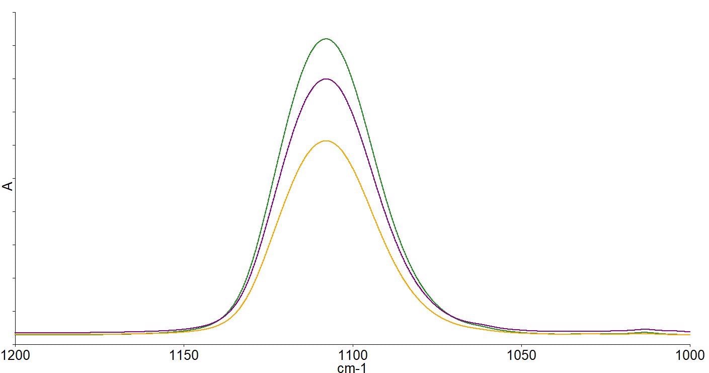
Figure 5. Spectra of high (green), medium (purple) and low (yellow) oxygen concentration wafers after subtraction of a zero oxygen reference FZ wafer spectrum. Image Credit: PerkinElmer, Inc.
The use of linear regression of a series of calibration standards or the use of standard calibration factors is facilitated by the calculation methods. In the past, standard reference materials of oxygen in silicon wafers were available for calibrations from NIST. Given that these are no longer available, most analyses now use the standard calibration factors.
Figure 6 shows the workflow for determining the carbon and oxygen content is as follows.
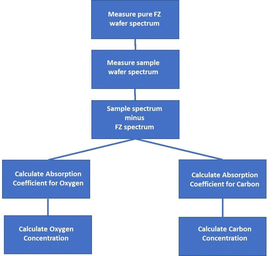
Figure 6. Carbon and Oxygen Content Determination Workflow. Image Credit: PerkinElmer, Inc.
Using the following calculation, the absorption coefficients for Oxygen and Carbon can be determined at the peaks 1107 cm-1 and 607 cm-1, respectively:
Absorption coefficient α = (1/d) Ln (T0 / T)
Where:
T0 is the calculated baseline transmission at the peak position
T is the measured transmission at the peak position
d is the sample thickness (cm)
The following formula is used to calculate the concentrations of oxygen and carbon in atoms/cm3 and parts per million atomic (ppma):
Oxygen atoms/cm3 = 3.14*1017 α
Oxygen ppma = 6.28 α
Carbon atoms/cm3 = 8.2x10¹⁶ α
Carbon ppma = 1.64 α
For the sample spectrum shown in Figure 4, the following values were calculated, as depicted in Table 1:
Table 1. Calculated values of Figure 4. Source: PerkinElmer, Inc.
| |
Oxygen |
Carbon |
| Absorption Coefficient, α |
2.61 |
0.384 |
| Atoms/cm3 |
8.1954 x 10¹⁷ |
3.1488 x 10¹⁶ |
| ppma |
16.3908 |
0.62976 |
The sample tested was a 6 inch CZ silicon wafer with a thickness of 500 microns, double-side polished (DSP) measured in Transmission.
Using the AutoPRO7 automation software, the concentrations of carbon and oxygen across the same wafer at the geometries shown in Figure 7 were mapped.
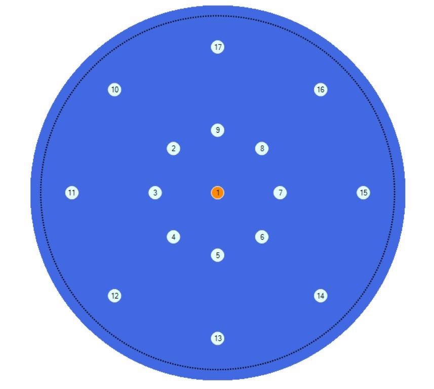
Figure 7. Geometry of the measurement positions in the Auto PRO7 software. Image Credit: PerkinElmer, Inc.
Spectra were collected automatically at the center of the wafer and at 20 and 50mm radii from the center at 45-degree increments, creating a total of 17 measurements across the wafer. The spectra are depicted in Figure 8.
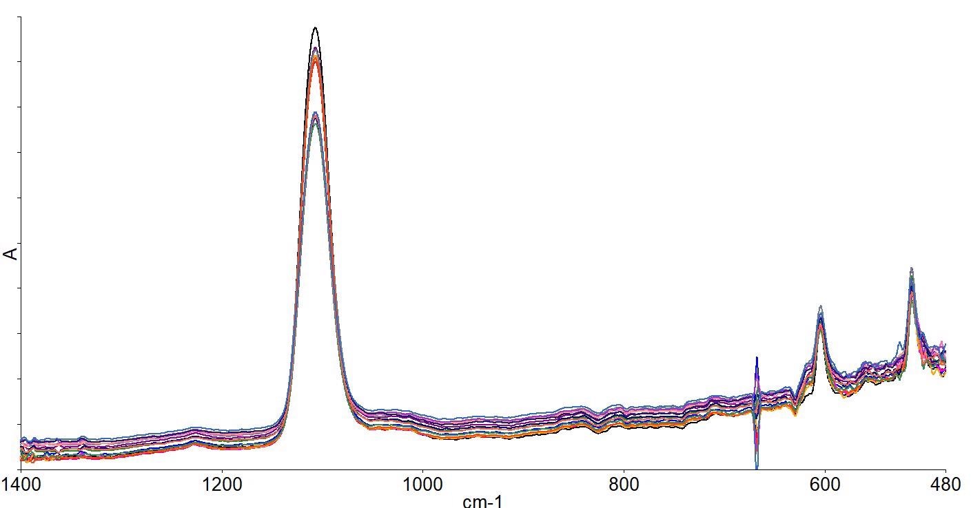
Figure 8. Spectra collected across the wafer. Image Credit: PerkinElmer, Inc.
The fact that there are different intensities in the oxygen peaks in the different measurements can clearly be seen. For each point, oxygen and carbon concentrations were calculated - shown in Table 2.
Table 2. Oxygen and carbon concentrations in the measured silicon wafer. Source: PerkinElmer, Inc.
| Sample Name |
Oxygen
Concentration
(atoms/cm3) |
Carbon
Concentration
(atoms/cm3) |
| 1115_B_001 |
8.21E+17 |
3.12E+16 |
| 1115_B_002 |
7.56E+17 |
2.96E+16 |
| 1115_B_003 |
7.59E+17 |
3.12E+16 |
| 1115_B_004 |
7.62E+17 |
3.08E+16 |
| 1115_B_005 |
7.64E+17 |
3.15E+16 |
| 1115_B_006 |
7.67E+17 |
3.27E+16 |
| 1115_B_007 |
7.60E+17 |
3.03E+16 |
| 1115_B_008 |
7.49E+17 |
3.44E+16 |
| 1115_B_009 |
7.60E+17 |
2.98E+16 |
| 1115_B_010 |
6.24E+17 |
3.03E+16 |
| 1115_B_011 |
6.19E+17 |
3.10E+16 |
| 1115_B_012 |
6.26E+17 |
2.79E+16 |
| 1115_B_013 |
6.18E+17 |
2.77E+16 |
| 1115_B_014 |
6.22E+17 |
2.96E+16 |
| 1115_B_015 |
6.26E+17 |
2.86E+16 |
| 1115_B_016 |
6.33E+17 |
2.93E+16 |
| 1115_B_017 |
6.18E+17 |
2.94E+16 |
| Mean Value |
6.99E+17 |
3.03E+16 |
| Std Dev |
7.53518E+16 |
1.67278E+15 |
| RSD% |
10.78% |
5.52% |
While the carbon measurements are comparatively consistent, the oxygen is shown to vary significantly across the wafer. To avoid inconsistencies when the wafers are cut into smaller individual pieces, the ideal wafer would have consistent measurements across its entirety.
Summary
It is clear that the PerkinElmer Spectrum 3 with MappIR wafer analysis system is capable of measuring the levels of impurities present in silicon wafers. This is a parameter that is crucial for the performance of the wafer.
With the use of macros in the software, the data collection and calculations can be automated, and the calculations can be customized according to the regulatory body method required.
Other semiconductor applications, such as the measurement of coatings and dielectrics as well as Epitaxial films, can also be conducted.
Raw materials identification in the semiconductor industry is also possible with the Spectrum 3, which can be coupled to a Spotlight FT-IR microscope for defect analysis.
References
- SEMI MF1188-1105 Test Method for Interstitial Oxygen Content of Silicon by Infrared Absorption with Short Baseline.
- SEMI MF1391-93 (Reapproved 2000) Test Method for Substitutional Atomic carbon Content of Silicon by Infrared Absorption.
- National Standards of the People's Republic of China GB 1557-89, GB/T 1558.
- JEITA EM-3503 Standard Test Method for Substitutional Atomic Carbon Content of Silicon by Infrared Absorption.

This information has been sourced, reviewed and adapted from materials provided by PerkinElmer.
For more information on this source, please visit PerkinElmer.