This article examines the use of femtosecond (fs) laser ablation for site-specific TEM sample preparation in a FIB-SEM. Various workflows are shown facilitating TEM lamella preparation of regions of interest (ROI) buried so deep into the sample that they cannot be directly accessed using FIB.
As a preferred and known method, the so-called Cut-to-ROI workflow was designed and is described in detail. Common limitations in the preparation of large TEM lamellas are examined, as well as the new potentialities that LaserFIB opens for microstructural characterization.
Lately, LaserFIB instruments have been attracting significant interest in the microscopy community. The term LaserFIB represents the fusion of a FIB-SEM with an ultra-short pulsed laser, usually an fs laser, within a single instrument.
The laser adds extra features to the FIB-SEM, extending its already wide application space.1 By means of fs laser ablation, significant volumes of material can be rapidly eliminated from a sample and, in most cases, with insignificant damage to the sample.
Thus, accessing regions of interest buried deep in the sample is now possible for their successive FIB-SEM analysis.
Other applications of LaserFIBs include the manufacture of micromechanical devices for materials testing with dimensions ranging in the millimeter scale,2,3 preparing surfaces for EBSD analysis4,5 and the making of pillar-shaped samples for the synchrotron or X-ray microscope.6
In the ZEISS Crossbeam laser – the LaserFIB assembly ZEISS implements – the laser work is conducted in a dedicated chamber to avoid contaminating the main FIB-SEM chamber by laser ablated debris.7
This article seeks to explore the possibilities offered by the ZEISS Crossbeam laser for TEM sample preparation. Various preparation workflows are presented as well as the discussion of potential modifications to adjust to particular microstructural characterization challenges.
The workflows are ideally suited for the TEM cross-section preparation of deeply buried features of concern or the preparation of several thinned windows that cover a large specimen area.
Experimental
All experiments were performed using a ZEISS Crossbeam laser. ZEISS Crossbeam laser is fitted with a diode pumped solid state (DPSS) 515 nm (green) laser with laser pulses of less than 350 fs duration.
Pulse repetition rates can be adjusted across a range of 0.1 kHz to 1 MHz. The maximum output power is 10 W when functioning at 1 MHz. This laser offers material removal rates in excess of 15 mio µm³/s in silicon, representative of at least three orders of magnitude enhancement in speed in comparison to any focused ion beam.1
When determining the laser milling strategy for a particular layout, key parameters include writing speed (in mm/s), laser power (in percentage), pulse repetition rate and number of passes (hatches). Users can input these for particular shapes or groups of shapes in a CAD interface.
ZEISS Crossbeam laser includes an Ion-sculptor gallium FIB column with beam currents of 1 pA to 100 nA. For the lamella lift-outs, an OP400 (Oxford Instruments plc) micromanipulator and a gas injection system (GIS) were employed.
For most of the experiments, the samples used were silicon, and for the H-bar experiment, a 99.9% pure copper foil was used. These materials were selected to highlight the different workflows because they are easily accessed, homogeneous and a good reference for comparative analysis with standard FIB work.
Chunking with the Laser
Figure 1 exhibits a laser prepared “macro-lamella,” also called a chunk, in silicon. The chunk was determined by performing a coarse milling step of two opposing boxes. One of these boxes is displayed schematically in Figure 1a as a shaded blue rectangle.
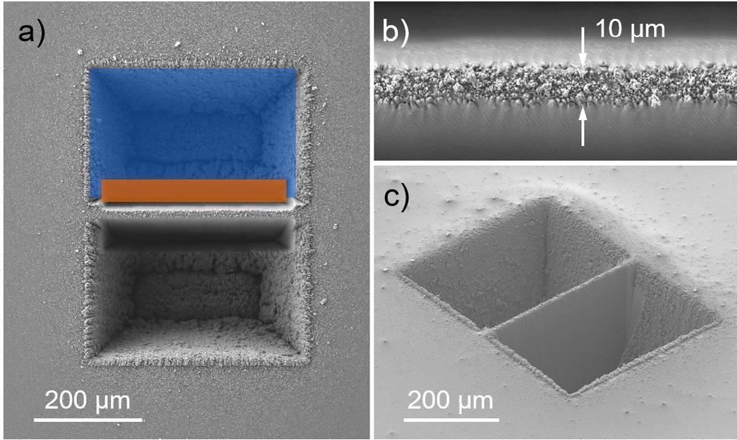
Figure 1. SEM images of a laser-machined chunk. a) Top view with laser milling shapes overlaid on one side of the chunk; blue for the rough milling and orange for the polishing step. b) Magnified top view. c) Sample tilted 54° and rotated. Image Credit: Carl Zeiss Microscopy GmbH
In the next laser machining step – signaled by the orange shaded rectangle – both sides of the chunk were polished. The coarse milling objects were 400 µm wide nominally. The ones used for the polishing step were 350 µm. The position of the boxes was selected to produce a chunk thickness of around 10 µm as measured at the top, as shown in Figure 1b.
Once the laser polishing step was completed, the sidewalls of the chunk demonstrated a taper of (7±1)°. The chunk preparation by laser is akin to conventional FIB preparation. The primary difference is the scale. The laser-prepared chunk’s dimensions are a factor of 10 to 20× larger than for a standard gallium FIB chunk.
Still, the laser fabrication process is extremely quick. For the chunk displayed in Figure 1, the total laser machining time was just 80 seconds.
To evaluate numerous ways to use the laser to support TEM sample preparation, an array of 3 × 2 chunks was prepared. This array is displayed in Figure 2. The entire array spans an area of 1.6 × 1.3 mm² and was patterned in 240 seconds.
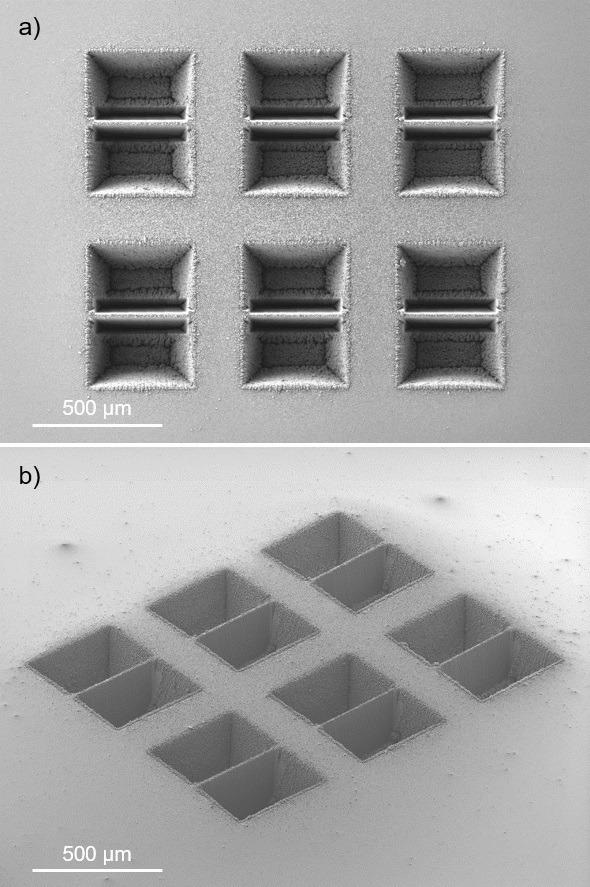
Figure 2. SEM images of a 3 × 2 array of laser-machined chunks. a) Top view. b) Sample tilted 54° and rotated. The FOV width is 2.3 mm for both images. Image Credit: Carl Zeiss Microscopy GmbH
Thinning and Shaping by FIB
Gallium FIB machining was employed once the laser preparation was complete in order to planarize and prepare the samples for lift-out. Various approaches were tested to examine their practicability. Figure 3 demonstrates the first example.
One of the laser-prepared chunks was thinned down to a little less than 2 µm across an area 58 µm wide and more than 75 µm deep by gallium FIB milling. This area looks bright when subjected to SEM imaging at 15 keV landing energy, Figure 3a.
The thinning of this lamella was performed in three steps conducted at FIB currents of 65 nA, 30 nA and 7 nA. When machining the front and back side, the sample was over-tilted and under-tilted, respectively.
The over- and under-tilt angles were reduced from 4° to 3° to 2° with decreasing milling current to guarantee a homogeneous thickness over the whole thinned window. The complete FIB thinning (including all three steps) took 3 hours in total. This is considered acceptable with respect to the sample size and the fact that the FIB milling can be completely automated.
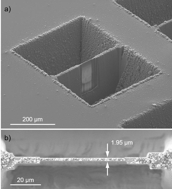
Figure 3. a) SEM images of a large FIB thinned lamella. a) Sample tilted 54° and rotated. b) Top view of the thinned region. Image Credit: Carl Zeiss Microscopy GmbH
For the following sample, an equal amount of time was invested to thin a 220 × 104 µm² area to 4.5 µm thickness including cutout, see Figures 4a and 4b. On this occasion, all FIB milling operations were performed at 65 nA with an over/under-tilt angle of 3°. Note, these settings would enable the production of a lamella of the dimensions shown in Figure 3 in under an hour.
As an alternative, the 3 hour time budget can be assigned just to the cut-out step of the as-lasered sample, without any FIB thinning/ polishing. This case is demonstrated in Figures 4c and 4d.
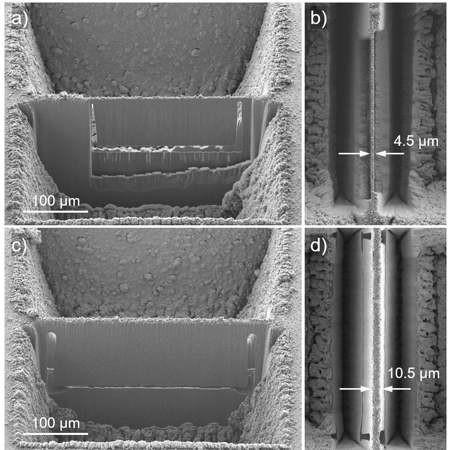
Figure 4. SEM images of two large lamellas after cut-out. a) and b) show different SEM perspectives – 0° and 45° stage tilt – of a 220 μm × 104 μm × 4.5 μm lamella. c) and d) show a bigger lamella with dimensions of 300 μm × 140 μm. This one is 10.5 μm thick at the top with a side wall taper of 7°. Image Credit: Carl Zeiss Microscopy GmbH
Again, a FIB current of 65 nA was applied. The sample is now 300 µm × 140 µm in size, with a thickness of 10.5 µm at the top and becomes thicker at the bottom as a result of the side wall taper of 7°.
Lift-Out
Despite their size, all three lamellas detailed in the previous section could be readily lifted out of the bulk sample and affixed to a 3 mm copper grid compatible with conventional TEM sample holders following the convention in situ lift-out procedure.8
For visual comparison, Figure 5a exhibits a standard-sized FIB lamella (15 µm × 14 µm), and Figures 5b to 5d demonstrate the lamellas from the experiments previously described, following the lift-out step. The FOV is the same for all four images in this figure.
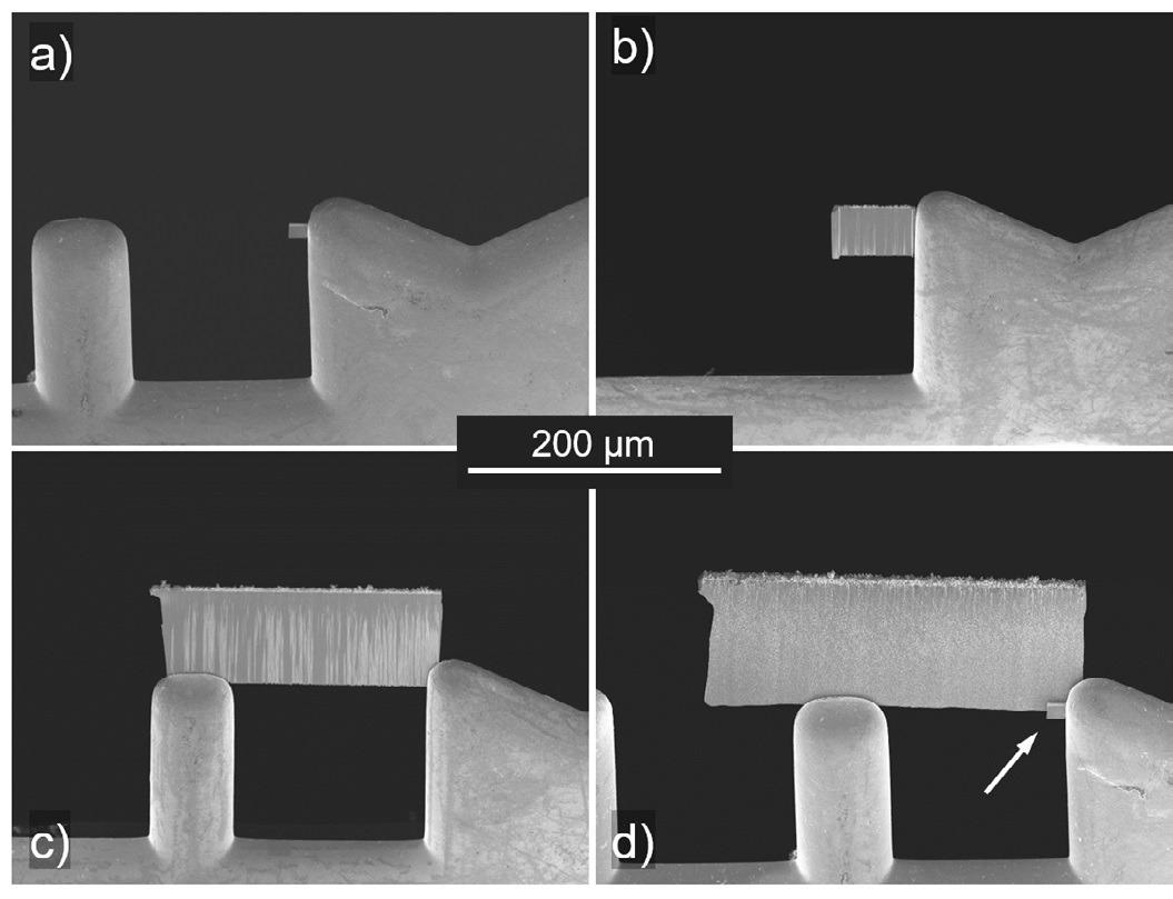
Figure 5. a) SEM image of a standard FIB lamella after in situ lift-out. b) to d) SEM images of laser prepared lamellas of increasing size after in situ lift-out. The lamella in d) was attached to the same grid as the lamella in a), which is highlighted by the arrow. Image Credit: Carl Zeiss Microscopy GmbH
Limitations
After the in situ lift-out, the next step includes thinning the lamella towards electron transparency. Very thin samples with a thickness of 100 nm or less are required for TEM analyses. It is at times challenging to acquire a uniformly thinned window of this thickness across a large area.
Contingent on the sample material, FIB-thinned windows are usually of the order of 10 µm × 10 µm or smaller. This is because the membrane starts to bend at a particular moment of the thinning process. This renders any additional thinning impossible without causing catastrophic damage to the sample.
The bending is a result of intrinsic stress release in the sample combined with its lower mechanical stability. Thus, the material itself places restrictions on what size can be acheived of an electron transparent window. Therefore, even in large chunks, only small windows may be thinned.
However, a number of small TEM windows can be prepared to cover a large specimen area.
The main application of the LaserFIB for TEM sample preparation was to offer three-dimensional (3D) site-specific preparation of structures of interest that are deeply buried. The following section details how this can be achieved using what has since been dubbed the ‘Cut-To-ROI workflow.’
The Cut-To-ROI Workflow
The start point or prerequisite of the Cut-To-ROI workflow is a laser-machined chunk. The chunk includes the ROI. Additionally, the position of the ROI in the depth of the chunk (direction of the bulk sample surface normal, Z) is determined.
The XYZ coordinates of a ROI can arise out of the sample layout itself (e.g. the already determined CAD layout of an electronics or semiconductor sample), from an earlier characterization by a nondestructive imaging technique (e.g. by X-ray microscopy),9 or any combination of both (e.g. lock-in thermography in combination with CAD chip layout).
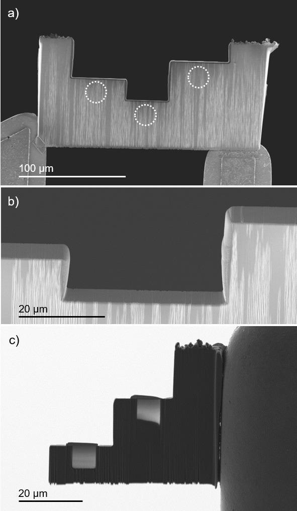
Figure 6. Laser processed lamella after FIB shaping to access ROIs 45 μm, 65, and 25 μm below the surface (dotted circles). b) The top surfaces after FIB milling are flat and smooth. c) SEM image at 5 kV of a different lamella after thinning of two ROIs. Image Credit: Carl Zeiss Microscopy GmbH
The laser can target any feature of interest located in the sample with an accuracy of about 2 µm.10 The chunk can be trimmed using FIB as displayed in Figure 6a. Here, the grid was rotated by 90° after the lift-out so that FIB incidence was at a right angle to the chunk side face for trimming.
Three ROIs were set at Z = 45, 65 and 25 µm, from left to right.
The FIB was used to take off the top of the chunk to form 40, 60 and 20 µm deep steps. It took 13 minutes to complete the three-step process at a FIB current of 30 nA.
Once trimming was complete, the grid was rotated back to the upright position. Figure 6b exhibits the top surface of one of the steps. The surface shown is flat and smooth, which allows the successive preparation of the TEM-thin areas by FIB.
Figure 6c demonstrates another excellent chunk after the final thinning of two ROIs 25 and 45 µm below the surface.
Figure 7 shows a variation of the Cut-To-ROI workflow. In this instance, the laser machined chunk was not removed from the bulk but was directly trimmed in the Z-dimension by FIB. For this purpose, the sample stage was at 0° tilt. The FIB trimming then takes place at an angle of 36° to the bulk sample surface (XY plane).
In this instance, the assumed ROI was at Z = 80 µm. The top 75 µm of the chunk were taken off over the full width of the chunk (65 nA FIB current, 1 hour 36 minutes FIB milling time), and then two standard FIB in situ lift-out specimens were prepared.
For the majority of applications, this alternative Cut-To-ROI workflow can be easily sped up by preparing a thinner chunk or even permitting some material removal from the top of the chunk by the laser beam tail.
Figure 7. a) Laser-processed chunk. After laser cutting, the top 75 μm were removed by FIB milling and two standard FIB lamellas were prepared. b) Detail of the right-most lamella corresponding to the area in the white frame in a). Image Credit: Carl Zeiss Microscopy GmbH
H-Bar Preparation by Laser
Another consideration would be to combine H-bar and Cut-To-ROI preparations.11 This method can be applied on small pieces of metal foils or wafers, for example. These pieces are fixed on edge for laser and FIB machining, as demonstrated in Figure 8.
Using the laser, two chunks were patterned into a 300 µm thick copper foil. The laser processing time for the larger chunk of 400 µm × 215 µm was just 34 seconds.
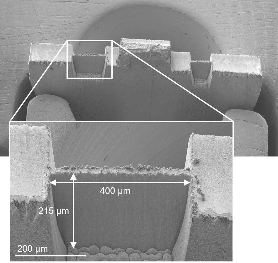
Figure 8. H-bar preparation in a piece of copper foil by laser. Two large H-bars were prepared. The one in the inset was machined in 34 seconds. Image Credit: Carl Zeiss Microscopy GmbH
Summary
This article discusses various workflows that combine laser and FIB machining for the preparation of TEM specimens. ZEISS Crossbeam laser systems facilitate 3D-site-specific preparation of regions of interest that are deeply buried or the preparation of several TEM-suitable windows covering a large sample area.
References
- F. Pérez-Willard et al., Expanding the application space of ion microscopy, submitted.
- M. J. Pfeifenberger et al., The use of femtosecond laser ablation as a novel tool for rapid micro-mechanical sample preparation, Materials and Design 121 (2017), pp 109-118.
- M. J. Pfeifenberger et al., Electron Irradiation Effects on Strength and Ductility of Polymer Foils Studied by Femtosecond LaserProcessed Micro-Tensile Specimens, Materials 12 (2019), pp. 1468-1483.
- M.P. Echlin et al., The TriBeam system: Femtosecond laser ablation in situ SEM, Mater. Charact. 100 (2015), pp 1-12.
- T. Schubert et al., Rapid Sample Preparation for EBSD-Analysis Enabled by the LaserFIB, ZEISS Application Note (2020), available online.
- B. Tordoff et al., The LaserFIB: New Application Opportunities Combining a High-Performance FIB-SEM with Femtosecond Laser Processing in a Second Integrated Chamber, Appl. Microsc. accepted.
- H. Doemer et al., Processing System, US8115180B2 (2012).
- L. A. Giannuzzi and F.A. Stevie, Introduction to Focused Ion Beams: Instrumentation, Theory, Techniques, and Practice, New York, Springer (2005).
- M. Kaestner et al. Novel Workflow for High-Resolution Imaging of Structures in Advanced 3D and Fan-Out Packages, 2019 China Semiconductor Technology International Conference (CSTIC) (2019), pp. 1-3.
- ZEISS Crossbeam Product Specifications, available on request at: www.zeiss.com/crossbeam
- J. Li, “Advanced Techniques in TEM Specimen Preparation”, in The Transmission Electron Microscope, Ed. Dr. K. Maaz, IntechOpen (2012).

This information has been sourced, reviewed and adapted from materials provided by Carl Zeiss Microscopy GmbH.
For more information on this source, please visit Carl Zeiss Microscopy GmbH.