In this interview AzoM talks to Dr Rosie Jones about the AZtecWave spectrometer, its features, applications, and its role in obtaining accurate results.
Can you explain what a Wave spectrometer is and in what industries are they primarily used?
The Wave spectrometer is an instrument for conducting elemental analysis by wavelength dispersive spectrometry on a scanning electron microscope. The WDS technique works on solid samples and can quantify the elements present in a sample at specific micron-size points or map the distribution of elements across a sample surface. In terms of where it is used, the Wave spectrometer is used in both industry and academia. It is primarily used in materials, metallurgy, geology, automotive and aerospace, and the energy sector. However, it can be useful in any field where the elemental composition of solid samples needs to be determined, particularly where elements are present in trace concentrations and these need to be accurately quantified.
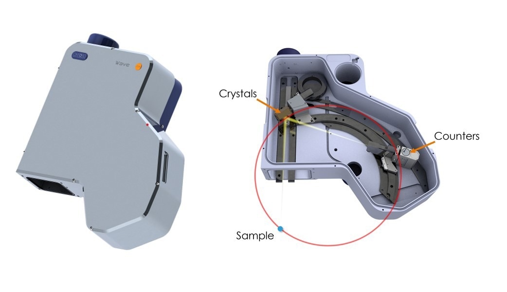 Image Credit: Oxford Instruments NanoAnalysis
Elemental analysis is typically carried out on the SEM using EDS, so how is WDS different and why would you want to add it?
Energy dispersive spectrometry (EDS) is an established technique for SEM compositional analysis.
EDS is fast and effective for determining elemental composition, but it does have some limitations that WDS can be used to overcome.
EDS determines and quantifies elements present in a sample based on the characteristic X-ray signal generated when an electron beam interacts with it. Different elements have characteristic X-rays with various energies, which occur as peaks in an EDS spectrum.
One limitation of EDS analysis is that some characteristic X-rays have very similar energies. With the spectral resolution of EDS, these occur as overlapping peaks in the EDS spectrum. For example, the Ti Kβ peak overlaps with the V Kα peak, making it difficult to accurately measure these elements if both appear in a sample. WDS has a higher spectral resolution, making it possible to resolve overlaps in the EDS spectrum with WDS, such as Ti Kβ and V Kα.
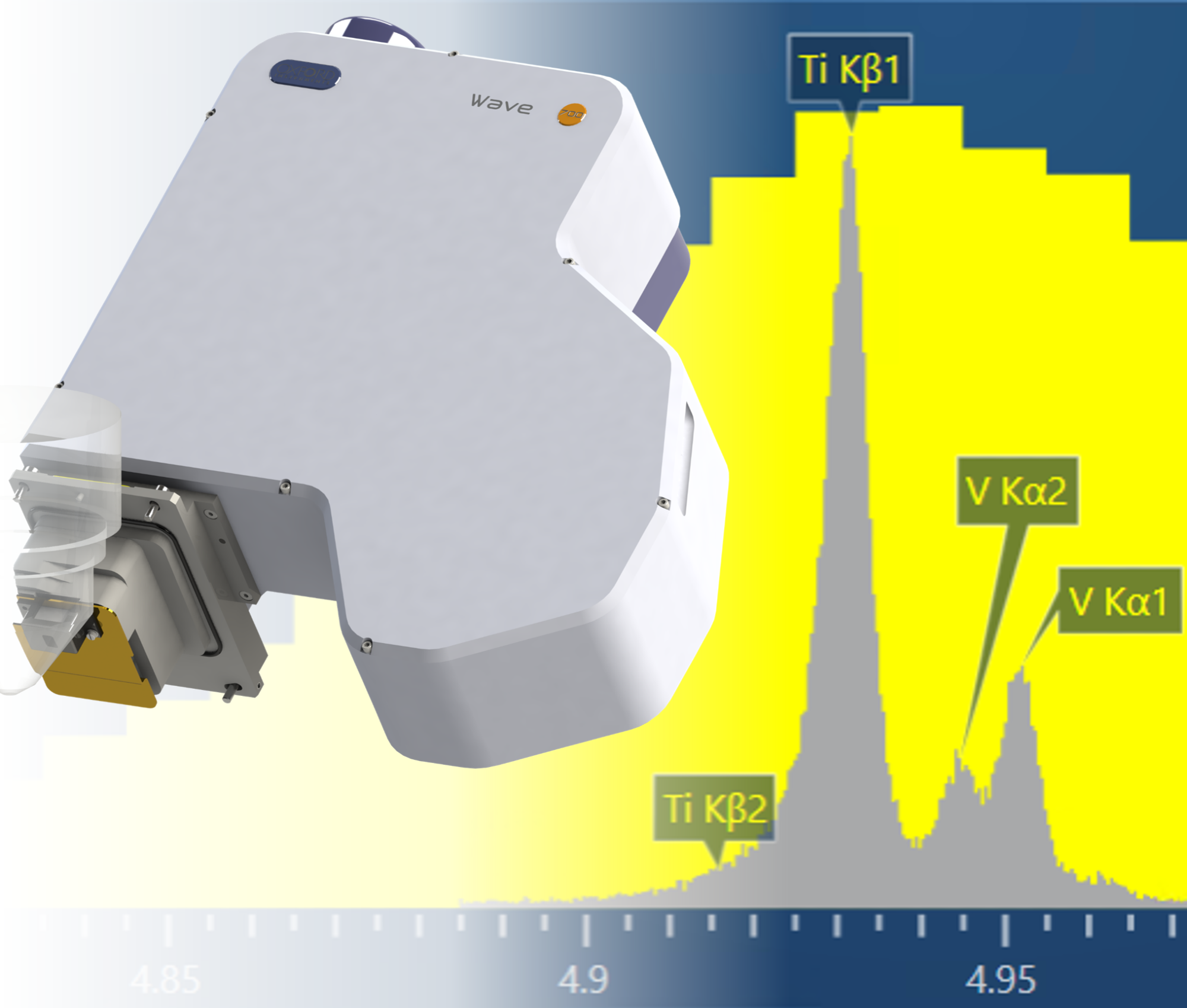
Image Credit: Oxford Instruments NanoAnalysis
Can you explain what the different styles of wavelength-dispersive spectrometers are?
There are two styles of wavelength dispersive spectrometers – Rowland circle and parallel beam. The primary difference between these two styles is geometry. The Wave spectrometer has Rowland circle geometry, the same geometry style used on an electron microprobe – the dedicated instrument for WDS analysis.
What advantages does the Rowland circle geometry of the Wave spectrometer bring?
The Wave spectrometer, which has a 210 mm Rowland circle and is fully focussing, delivers the best spectral resolution available. The resolution that can be achieved is approximately 10x higher than energy dispersive spectrometry (EDS) and 2x higher than what can be achieved with a parallel beam WD spectrometer.
This means that the Wave spectrometer can be used to separate characteristic X-ray peaks that EDS or other spectrometers cannot separate. Consequently, the Wave spectrometer brings certainty to element identification and more accurate quantification of elements affected by peak overlaps. The higher spectral resolution of the Wave spectrometer gives higher peak-to-background ratios and therefore lower detection limits. The Wave spectrometer can accurately detect and measure trace elements (<1000 ppm).
How does the Wave spectrometer offer a higher spectral resolution?
This is delivered through a combination of the physical geometry and size of the Rowland circle, and the use of a variable entrance slit positioned in front of the X-ray counters. The entrance slit optimizes the resolution and a narrower slit width increases the resolution that can be achieved.
What makes the positioning design of the Oxford Instruments Wave spectrometer unique?
The Wave spectrometer is positioned at an inclined angle on the SEM, not vertical, as is used on electron microprobes (i.e. EPMA). Having the spectrometer at an inclined angle on the SEM broadens the plane of the Rowland circle and brings position advantages to the sample in the SEM.
What advantages does this provide?
The sample height does not have to be so carefully positioned to generate accurate quantitative data. The sample height can vary up to about +/-0.5 mm without the sample moving off the Rowland circle. Therefore, there is no impact on count rates with slight variations in height. Consequently, the height of the sample can be adequately positioned simply using the secondary electron image on the SEM.
How does sample set-up compare to other alternatives?
It ultimately makes the sample set-up quicker and easier. Parallel beam WD spectrometers often have to go through focussing routines to ensure that the correct geometry is achieved for each element, lengthening analysis time. The sample must be very carefully positioned and focused on electron microprobes using the optical image, which also takes time.
Why is WDS a slower technique than EDS, and why does this matter?
Like EDS, WDS utilizes the X-ray signal generated by bombarding a solid sample with a beam of high-energy electrons. Unlike EDS, WDS is based on Bragg’s Law of diffraction and therefore can only measure X-rays of a single wavelength or energy at a time.
On the other hand, EDS measures all X-ray energies simultaneously, making it much faster for multi-element samples.
EDS typically has a higher solid angle and count rate, making EDS analysis quicker than WDS analysis. This is why we have designed our system and software so that users can simultaneously perform and combine EDS and WDS analysis – EDS can be used to quickly and accurately analyze major elements and those unaffected by peak overlaps.
WDS can be used just where needed to measure trace elements or those affected by peak overlaps in the EDS spectrum. The EDS and WDS analysis results are automatically combined in our AZtecWave software.
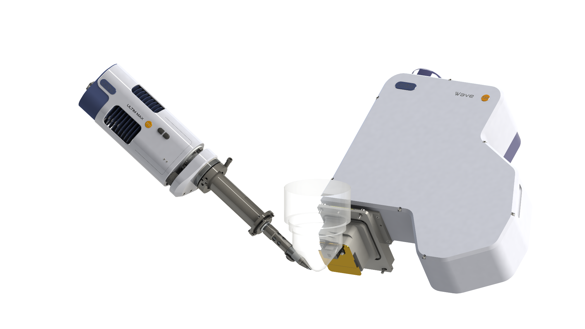
Image Credit: Oxford Instruments NanoAnalysis
What makes the Oxford Instruments Wave spectrometer easy to use?
The Wave spectrometer is fully controlled using the AZtecWave software. Because of some of the complexity involved with setting up WDS analysis, we have designed the AZtecWave software with a strong focus on ease of use. The user does not have to be an expert to use the system and achieve accurate results. For example, we have designed unique workflows not just for EDS or WDS analysis but to effectively combine both. We have also developed software technology that automatically optimizes the collection settings, instead of just applying default values or relying on inputs from the user that require expertise.
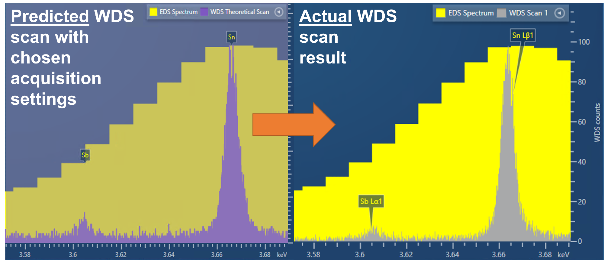
Image Credit: Oxford Instruments NanoAnalysis
What are some of the ease-of-use features of the system that consumers can take advantage of?
There are lots of ease-of-use features in the AZtecWave software. A significant development we have introduced to AZtecWave is the software technology I have just mentioned. This automatically takes the live input from both the SEM and EDS detector and uses it to automatically set the collection settings for the WDS analysis. For example, AZtecWave will automatically pick the most appropriate X-ray line and crystal, set the peak and background counting times to achieve a certain level of error on the analysis, and automatically set the background positions to avoid any interferences. These are difficult settings for a user to set without a good level of prior knowledge.
AZtecWave removes the complexity for the novice user, but it remains flexible for the expert user with options for manual selections/adjustments.
Other ease-of-use features include:
- Guided workflows for combining WDS with EDS analysis
- Step-by-step instructions in the user interface throughout the setup and data collection
- Inbuilt spectrometer performance checks to make sure that the Wave spectrometer is set up and performing correctly before data acquisition
- Help videos that can be easily accessed from the software for additional guidance
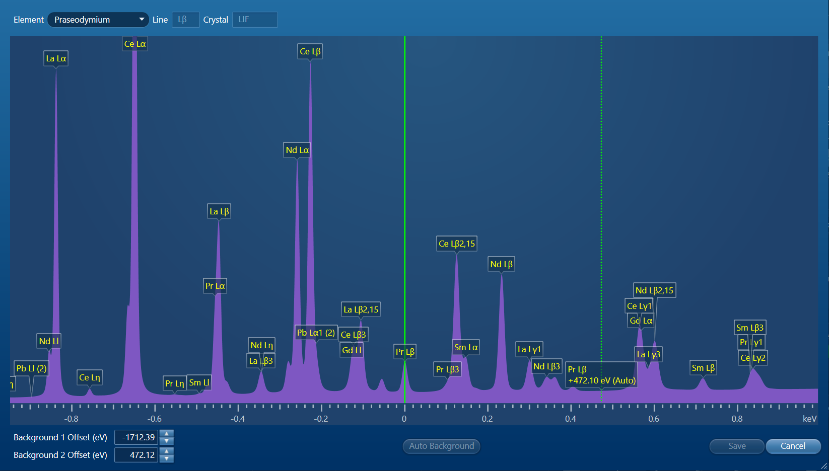
Image Credit: Oxford Instruments NanoAnalysis
Can you give specific application examples of what WDS and AZtecWave are used for?
WDS and AZtecWave can quantitively measure major, minor and trace elements in solid samples such as minerals, ceramics, and metals.
In geology, the trace element concentration of minerals can be used to interpret how they formed. In metallurgy, trace concentrations of elements such as carbon, sulfur, and boron can profoundly impact the metal's properties; therefore, it is important to quantify them accurately.
My colleague has recently carried out some work using WDS and AZtecWave to investigate the concentrations of dopants in semiconductor samples (https://www.oxinst.com/blogs/wds-sem-approach-for-studying-doping-in-semiconductors?business=nanoanalysis&sbms=nanoanalysis).
The analysis of rare earth elements (REE) is another important application that can be addressed using WDS and AZtecWave. The REE have numerous peak overlaps in the EDS spectrum, but these can be resolved using WDS. REE are increasingly being used in existing and developing technologies, such as fuel cells, electric vehicles, and batteries.
About Dr Rosie Jones

Dr Rosie Jones graduated with a BSc and MSc in GeoSciences and Geochemistry from the University of Leeds, and a PhD in Geology from the University of Edinburgh. She joined Oxford Instruments in 2019 after completing a Postdoctoral Research position at the University of Oxford. Rosie has always worked with a strong focus on (micro)analytical techniques, including SEM-EDS, EPMA-WDS, XRF and mass spectrometry. She is currently Product Manager for WDS and works within the X-Ray Products Team.

This information has been sourced, reviewed and adapted from materials provided by Oxford Instruments NanoAnalysis.
For more information on this source, please visit Oxford Instruments NanoAnalysis.
Disclaimer: The views expressed here are those of the interviewee and do not necessarily represent the views of AZoM.com Limited (T/A) AZoNetwork, the owner and operator of this website. This disclaimer forms part of the Terms and Conditions of use of this website.