Semiconductor devices are now universal and have a critical role in modern-day society. Semiconductors influence how we provide entertainment, interact and communicate with the world, and enable many modern conveniences. As more services and products become connected, semiconductor devices have developed into a strategic priority, allowing development needs to evolve and prevent supply disruptions.
To meet the growing demands, scaling up has been pushed to the limit by device manufacturers while new materials and processes have been introduced, facilitating the necessary material innovations for integral semiconductor equipment.
Semiconductor manufacturing can be separated into two halves; the “front-end”, which focuses on wafer fabrication, and the “back-end”, where integrated circuits are assembled. The manufacturing process requires very high precision using the best equipment.
This article discusses the differences between the two processes, some sealing solutions needed for back-end semiconductor processing, and their benefits. Many demanding applications require processes where the equipment is optimized to provide the highest yields possible at the lowest cost possible.
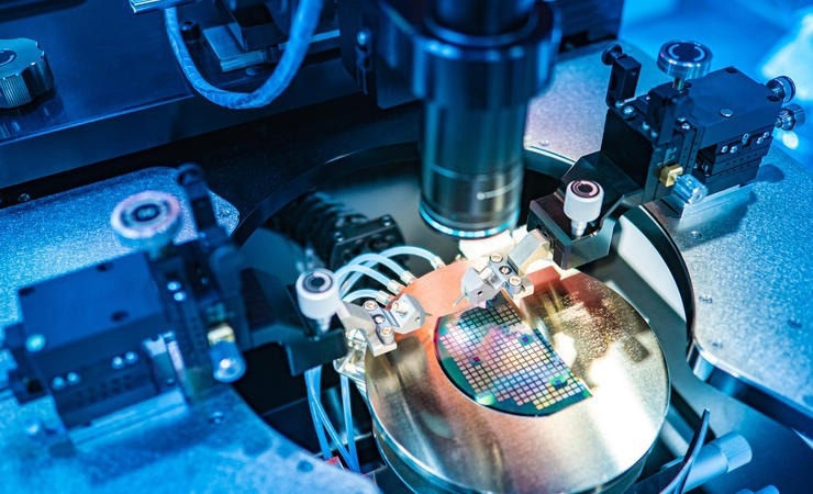
Image Credit: Omniseal Solutions™
Brief Overview of Front-End Semiconductor Manufacturing
The front-end process involves numerous complex steps to transform a wafer into a finished device. This process requires oxidation, wafer cleaning, photolithography to pattern devices, and deposition, etching, doping, and metallization steps.
For process control, metrology and inspection equipment are also used. At this point, the wafers are inspected for irregularities that may cause issues with the end product. Optical techniques are used, and e-beam inspection is often required to find the smallest defects.
Omniseal Solutions' high-performance seals are used throughout the manufacturing process and perform in challenging conditions, such as aggressive chemical and plasma environments and high temperature and ultra-high vacuum conditions.
An array of applications comprises a broad range of chemical vapor deposition, CVD, and plasma etch equipment. As well as the front-end process, we also provide precision solutions for the back-end process.
Key Processes in Back-End Semiconductor Manufacturing
Wafer probe
This is the point in semiconductor manufacturing where devices are tested to determine whether they fit design specifications.
While still on the wafer, the semiconductors are tested using micro contacts with the circuits. Probes then measure and translate signal responses. Any semiconductors that fail are either repaired or discarded.
Wafer dicing
Wafer dicing is the process of slicing a semiconductor into individual die. Traditionally, this would be carried out by saw dicing. Recently, there has been a significant shift to smaller and thinner semiconductor chips, developing new techniques such as laser dicing.
Die bond
The individual die are too fragile and intricate to be handled on their own and must be safeguarded.
The Die Bond process secures the die to the substrate. The substrate then acts as the interface between the electronics manufacturing macroscopic scale and the chip’s microscopic scale.
Wire bonding
The next step is a wire bond process. This process forms an electrical connection by fixing each pad on the die with one on the substrate using a wire. Techniques such as flip chip can also be used.
Encapsulation
The bonded die and frame must be sealed to complete the back-end semiconductor processing. This can be achieved by attaching a sealed lid or using a molded plastic compound. At this point, the semiconductor part is ready to be used in electronics manufacturing. Final testing can be done before shipping the completed chip.
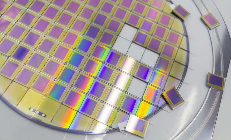
Image Credit: Omniseal Solutions™
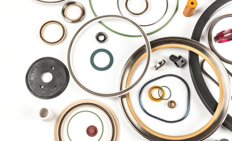
Image Credit: Omniseal Solutions™
Semiconductor Sealing and Material Solutions from Omniseal Solutions™
Omniseal Solutions™ manufactures and engineers high-performance wear and sealing solutions that are an essential part of the above back-end semiconductor manufacturing processes. These include various precision equipment, such as the SMT Dispensing and Pick & Place Test Handlers. Omniseal Solutions™ provides products and services that address challenges in the testing and assembly processes of back-end manufacturing.
The company’s global business is agile, providing custom solutions across the semiconductor value chain.
Omniseal Solutions™ provides rapid prototyping, where the design team produces a prototype and a solution engineered to the strictest of tolerances.
The Omniseal® polymer, spring-energized seals and metal face seals are effective sealing options, as they deliver on the critical requirements of the equipment industry, such as withstanding extreme pressures and temperatures and resisting corrosive chemicals and other aggressive media.
The company also offers custom machined parts, such as CMP retaining rings and Meldin® polyimide solutions for bearings, clamp rings, and custom components.
Other benefits include:
- Low friction and wear
- Electrical insulation
- Low outgassing and high purity
- Less maintenance and downtime
The company’s semiconductor and electronics experts are available to help with application challenges. Contact the team today.
Acknowledgments
Produced from material originally authored by Thomas La Tempa from Omniseal Solutions™

This information has been sourced, reviewed and adapted from materials provided by Omniseal Solutions™.
For more information on this source, please visit Omniseal Solutions™.