These photovoltaic (PV) cells are constructed based on the distinctive structure of the perovskite crystal, often symbolized as ABX3, with CaTiO3 as a natural example.
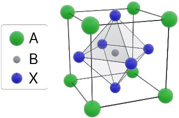
Figure 1. Perovskite crystal example. Image Credit: Semilab Semiconductor Physics Laboratory
Organic-inorganic hybrid perovskites, derived from the ABX3 arrangement, have emerged as promising materials for high-performance solar cells. In these hybrids, the A-site can include monovalent cations like methylammonium (CH3NH3+), formamidinium (HC(NH2)2+), or cesium (Cs+).
Meanwhile, the B-site can accommodate either lead (Pb2+) or antimony (Sb2+), and the X-site can be filled with halogen ions such as chlorine (Cl-), iodine (I-), or bromine (Br-).
Metrology
Spectroscopic ellipsometry (SE) is a useful method for analyzing different layers within the solar cell structure.
The Semilab SE-2000 can cover wavelengths from 190 nm to 25 μm. The thicknesses of layers and the optical dispersion of layer materials are determined by modeling the layer structure and adjusting the model parameters to align the simulated spectra with the measured ones.
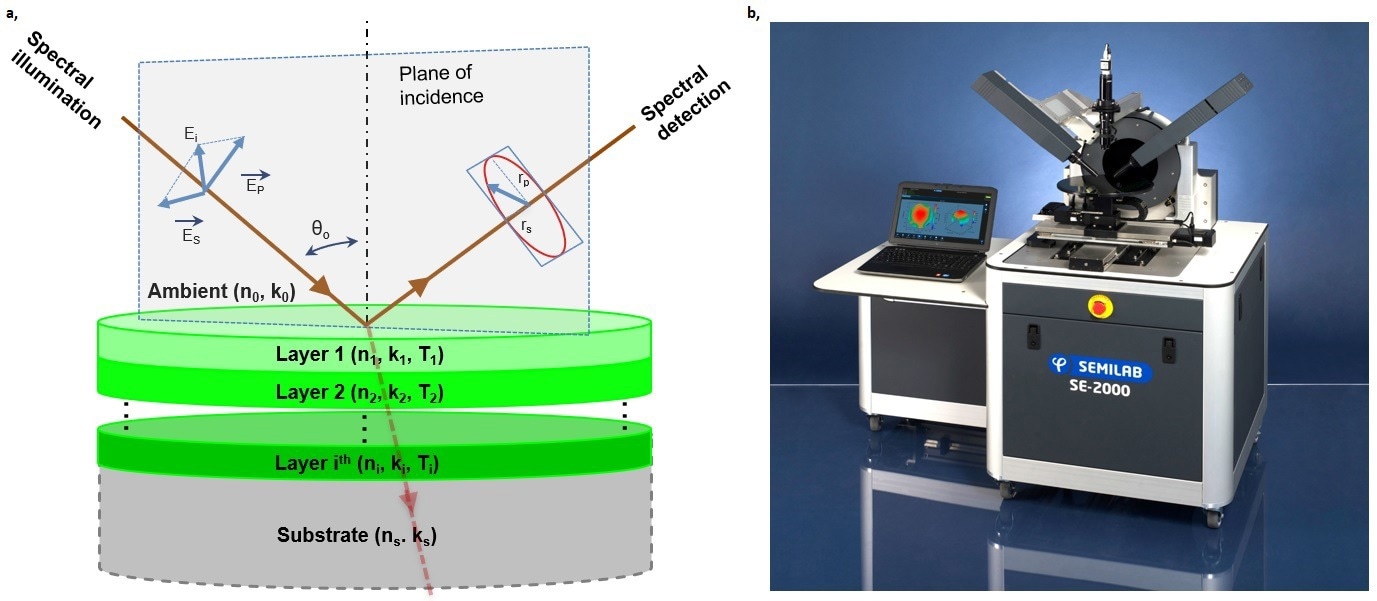
Figure 2. (a) Schematic view of ellipsometry principle; (b) SE-2000 metrology system. Image Credit: Semilab Semiconductor Physics Laboratory
Use Case
This investigation employed ellipsometry to analyze a series of samples prepared on glass substrates measuring 10×10 cm2, including:
- Single perovskite layer
- Perovskite layer in a stack configuration.
A single perovskite layer on glass was an excellent reference sample for subsequent measurements of the perovskite layer in a stacked configuration.
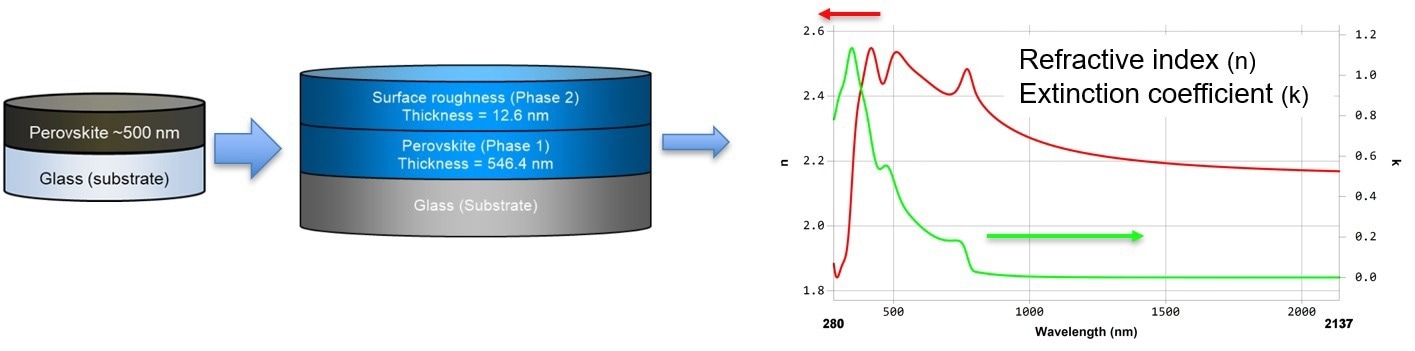
Figure 3. Investigation of single perovskite layer. Image Credit: Semilab Semiconductor Physics Laboratory
The perovskite layer in a stacked configuration exhibited slight distinctions compared to the measurement of a single perovskite layer. These differences can be attributed to factors such as varying crystal sizes and defects within the stack.
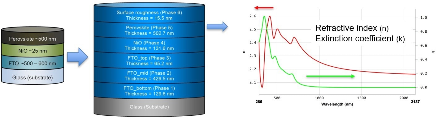
Figure 4. Perovskite layer in a stack configuration. Image Credit: Semilab Semiconductor Physics Laboratory
By analyzing the extinction coefficient, the complete spectrum of the typical OPD* can be unveiled (Figure 5). The optical characteristics of perovskite materials can be harnessed to produce a band gap map (Figure 6).
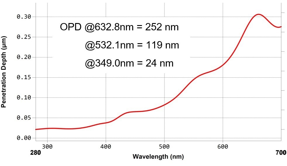
Figure 5. *Optical penetration depth in perovskite layer. Image Credit: Semilab Semiconductor Physics Laboratory
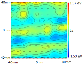
Figure 6. Band gap map. Image Credit: Semilab Semiconductor Physics Laboratory
UV Irradiation Effects
Perovskite materials are widely recognized for their sensitivity to ultraviolet (UV) light.
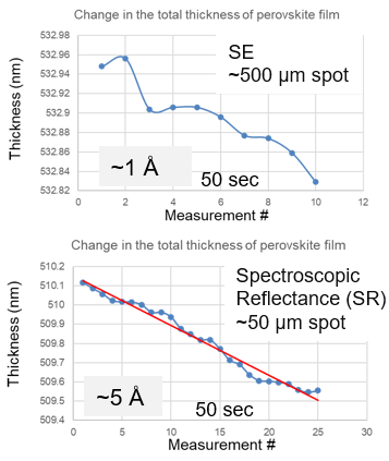
Figure 7. UV irradiation effects. Image Credit: Semilab Semiconductor Physics Laboratory
Long-Term Stability Investigation
After six months, several alterations were discernible in the optical spectra of the perovskite material.
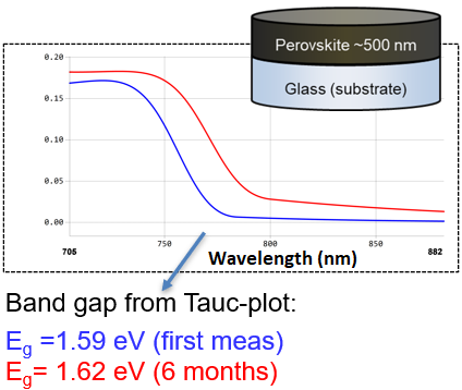
Figure 8. Long term stability test. Image Credit: Semilab Semiconductor Physics Laboratory
Materials and Structures
Complex perovskite materials possessing the ABX3 formulation, wherein A signifies an organic/inorganic cation, B represents a metal cation, and X symbolizes an anion.
References and Further Reading
Giles E. Eperon et al. Formamidinium lead trihalide: a broadly tunable perovskite for efficient planar heterojunction solar cells. Energy & Environmental Science, Volume 7, Issue 3, March 2014, Pages 982-988, doi: 10.1039/c3ee43822h.

This information has been sourced, reviewed and adapted from materials provided by Semilab Semiconductor Physics Laboratory.
For more information on this source, please visit Semilab Semiconductor Physics Laboratory.