In this interview, Dr. Stuart Wright, a Senior Scientist at Gatan/EDAX, talks to AZoMaterials about the versatile applications of Electron Backscatter Diffraction (EBSD) in materials science and metallurgy.
Can you provide an overview of the versatile applications of EBSD in materials science and metallurgy?
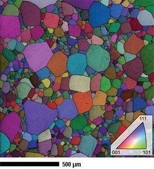
EBSD is a versatile and indispensable tool in materials science and metallurgy, suitable for a broad range of applications. One of its key roles is in microstructure analysis, allowing researchers to delve deep into the internal arrangement of materials. By providing valuable insights into grain size, grain orientation, and phase identification, EBSD aids in characterizing materials' properties and behaviors, making it an essential component in quality control and materials development.
This technique has been successfully employed in various materials, from traditional metals and semiconductors to advanced ceramics and even biomaterials. Researchers and engineers leverage EBSD to gain an intimate understanding of these materials at the microstructural level, which is invaluable for tailoring materials to specific industrial needs.
EBSD image quality and IPF orientation map from beam-sensitive MAPI perovskites collected a 10 kV, 150 pA beam dose.
Image Credit: Gatan, Inc.
Texture analysis is another pivotal application of EBSD. It is instrumental in studying the preferred crystallographic orientations within materials, a crucial factor in the automotive, aerospace, and manufacturing industries. By providing detailed insights into crystallographic textures, EBSD assists in optimizing materials for improved performance and manufacturability. Moreover, EBSD plays a significant role in investigating stress and deformation effects in materials. Researchers can precisely analyze the subtle changes in orientation within the microstructure, providing vital information for understanding the mechanical properties of materials under various conditions.
The influence of EBSD extends into the earth sciences, enabling the examination of minerals and rocks. I have seen fascinating EBSD studies of fossils that provide insight into the nature of prehistoric creatures, such as EBSD studies comparing the microstructure of modern birds' eggs with the eggs of dinosaurs.
EBSD is an incredibly versatile tool with a broad spectrum of applications, making it an indispensable asset in materials science, metallurgy, and earth sciences. It continues to drive innovation, research, and the development of materials tailored to meet the ever-evolving needs of modern technology and industry.
Across different materials such as metals, ceramics, and biomaterials, could you share some specific applications of EBSD that you find particularly noteworthy?
In materials engineered for specific applications, whether metals or ceramics, EBSD's versatility makes it a particularly valuable tool for studying complex microstructures and understanding the mechanisms behind forming different phases, grain sizes, and textures. Increasing our understanding of microstructure has a two-fold interrelated benefit for materials science. First, we know microstructure plays a vital role in material behavior, whether mechanical, chemical, electrical, or any other type of property or combination of properties. The better we understand the role of microstructure on a material's response to the environmental conditions it is designed for, the better we can predict that response and the better we can engineer a material to improve performance. For example, tolerances can be tightened due to better predictive capabilities. Tighter tolerances lead to, for instance, lighter-weight automobile components. The second benefit of increasing our understanding of microstructure is optimizing the forming processes of materials. EBSD has improved our insight into the evolution of microstructure during forming. Understanding the evolution of microstructure dramatically enhances our ability to optimize the forming process to achieve the best microstructure possible for a given engineering application and minimize the amount of forming steps and energy expended to create a component. For instance, EBSD has been in the aerospace industry to optimize the performance of superalloys for gas turbine engines, which operate under high-temperature and high-stress conditions.
EBSD is pivotal in developing advanced materials like shape memory alloys, where the precise orientation of the crystal lattice greatly influences their unique properties.
Moving on to ceramics, EBSD plays a crucial role in studying polycrystalline materials. It aids in the design of piezoelectric ceramics used in electronic devices, where the orientation of domains within grains significantly impacts their electrical properties. Furthermore, EBSD has applications in structural ceramics, such as in examining grain boundaries in silicon carbide for high-temperature structural materials or in the characterization of the crystallographic orientation of ceramics used in thermal barrier coatings for gas turbine engines.

Image Credit: Shutterstock.com/asharkyu
In biomaterial research, EBSD's potential is just beginning to be realized. By examining the crystallography of biomaterials, we can gain insights into the interaction of the microstructure of implant materials with the host environment, potentially contributing to the development of better implants and prosthetics.
Can you elaborate on why obtaining a polished, scratch-free surface is essential and the impact of improper preparation?
Sample preparation in EBSD analysis plays a pivotal role in the quality and accuracy of the results obtained. To understand why a polished, scratch-free surface is essential, we must first recognize that EBSD captures the crystallographic information from the material's topmost surface layers. Therefore, even minor imperfections on the surface, such as scratches, deformations, or irregularities, can significantly impact the quality of the EBSD patterns and, by extension, the analysis results.
When the sample surface is not prepared adequately and contains scratches or deformations, it can introduce unwanted variations in the acquired patterns. For instance, scratches can lead to deviations from the ideal crystallographic orientation and hinder the EBSD software's ability to identify and index the patterns to specific crystallographic phases correctly. Sometimes, the patterns may become so distorted that they cannot be indexed, rendering the analysis ineffective.
Improper sample preparation can result in the collection of patterns that are composites of multiple grains rather than a reflection of a single, well-defined grain. This can lead to difficulty in determining the material's microstructure, including grain size, orientation, and texture.
While the quality of patterns is the focus of sample preparation because indexing success is vital to achieving good EBSD results, another important consideration applies to most microstructure imaging modalities. When we characterize the microstructure at the surface of a sample, we generally assume that the microstructure is representative of the material in the bulk below the surface we are looking at. If our sample preparation modifies the surface through, for example, mechanical deformation or significant localized heating, then we may unduly stretch the assumption that the surface microstructure is representative of the bulk. As our indexing routines continue improving, this should not impact the need to prepare samples properly.
When considering EBSD mapping, what factors and considerations guide you in determining the appropriate step size for analysis?
Choosing an appropriate step size for EBSD mapping involves several nuanced factors. First and foremost, the specific goals of your analysis play a pivotal role. If the primary objective is to determine accurate grain size statistics, a basic guideline is to aim for a minimum of 25 data points per average grain.
In contemporary EBSD systems, there has been a notable improvement in data acquisition speed, allowing us to increase the density of acquired data points significantly. In some cases, we now routinely collect over a thousand data points per grain, especially for applications focused on texture analysis. This high point density can provide a more comprehensive understanding of grain orientation and microstructural variations.
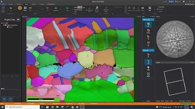
EBSD mapping example from a high entropy alloy weld.
Image Credit: Gatan, Inc.
However, suppose your analysis aims to examine finer microstructural features such as grain boundaries, defects, or orientation gradients within grains showing material flow during plastic deformation. In that case, you may need an even higher point density. In these situations, a smaller step size is recommended to ensure that the EBSD system accurately captures the microstructure's intricacies.
Conversely, for applications like mapping the spatial distribution of constituent phases or in texture analysis, the focus is not primarily on grain-level details, and you can afford to use a larger step size. This larger step size speeds up data acquisition and ensures that you have sufficient data points to achieve your goals. Of course, a small enough step size to see, at least, a coarse reconstruction of the microstructure can be helpful if there is an uncertainty in the quality of the EBSD indexing. I would add a word of caution in the use of EBSD for the measurement of texture. Texture is essentially a statistical measure of the preferred crystallographic orientation of grains in a polycrystal. EBSD is an excellent tool for measuring texture. Still, unfortunately, I too often see a significant misunderstanding of the role of sampling when characterizing polycrystalline materials with EBSD for texture analysis. The critical factor to achieving statistical reliability in texture measurements is not the number of individual EBSD measurements but rather the number of grain orientations sampled. For example, 1000 measurements at a step size coarser than the grain size covering a large area will give a much more accurate texture measurement than one million measurements covering just a few grains.
Another significant factor influencing the choice of step size is the nature of the material under investigation. For example, coarse-grained materials may require a different step size than fine-grained or multi-phase materials. It is crucial to adapt your step size to suit the characteristics of the material and your specific research objectives.
EBSD patterns are vital, but what factors can cause patterns to become weak or challenging, and how do you address such issues?
EBSD patterns are indeed the backbone of our technique, but certain factors can make them challenging to work with. As I’ve already mentioned, the quality of the sample surface can be a critical factor in the quality of the patterns; thus, sample preparation is vital. A polished, scratch-free surface will provide the highest quality patterns, as any deformations or contamination on the sample surface will degrade the patterns. Additionally, rough surfaces, fractures, or the presence of pores or voids can lead to weak or shadowed patterns. It is possible to get patterns from rough or fractured surfaces. It can be difficult, but sometimes, it is critical to characterize the surface without any disturbance due to sample preparation. With a bit of patience, this can often be achieved. In these cases, I recommend recording EBSD patterns during the mapping without any image processing applied. The recorded patterns can then be imported into our offline software to take advantage of the more advanced image processing and indexing capabilities available without wasting valuable SEM time.
To create a clean surface, these issues can be addressed through careful sample preparation, including mechanical, chemical, or ion polishing. Another challenge can arise from beam-sensitive materials that can be damaged under the electron beam. In such cases, using a lower acceleration voltage and employing rapid data collection strategies can help mitigate damage and capture usable patterns.
Could you explain the technique EBSD employs to investigate residual stress within materials, especially when dealing with cases of plastic deformation?
Investigating residual stress, especially in cases of plastic deformation, is a significant application of EBSD. When we study materials using EBSD, we capture microstructural information that extends beyond just grain orientation. We can also measure lattice strain within individual grains by analyzing the changes in crystallographic orientation at a very fine scale.
In the EBSD analysis, we rely on capturing the subtle changes in orientation, typically less than a degree, which indicate plastic deformation within the material. By studying these fine changes, we can deduce the geometrically necessary dislocation density, a key parameter in characterizing the residual stresses within the material. Cross-correlation techniques are used to precisely characterize subpixel differences between patterns from neighboring points on the sampling grid for even more precision. As a result, we can determine the deformation tensor, which provides insights into the residual stresses present in the material. With this technique, we are not just looking at the average stress; instead, we can map the variations in stress within the microstructure. This is particularly valuable in understanding how materials behave under load, helping us improve our knowledge of their mechanical properties and performance in real-world applications.
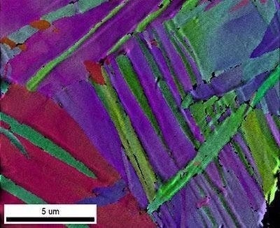
EBSD image quality and IPF orientation map from cryo-forged nanotwinned titanium collected at 7 kV and 200 pA beam dose for improved spatial resolution.
Image Credit: Gatan, Inc.
It is essential to remember that EBSD is a surface technique. While we cannot measure stresses deep within the material, we can provide valuable insights into the microstructural effects of plastic deformation. In this way, EBSD contributes significantly to our understanding of materials' mechanical behaviors and helps researchers and engineers make more informed decisions regarding their use.
Can you provide details on how the Clarity detector works and its advantages in EBSD analysis?
The EDAX Clarity detector represents a significant advancement in EBSD pattern collection and analysis, offering a range of advantages for researchers. One of its key features is its direct detection capability, which fundamentally changes the way EBSD data is collected. Instead of relying on a phosphor screen to convert electrons into visible light, the Clarity detector counts electrons directly. By removing multiple noise sources and inefficiencies in the pattern collection process, this approach drastically enhances the detector's sensitivity, making it exceptionally useful in scenarios where traditional phosphor screens fall short.
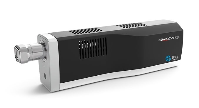
Image Credit: Gatan, Inc.
The main advantages of the Clarity detector are its versatility and the quality of data it produces. It is especially beneficial when working with low beam voltages, often necessary for beam-sensitive materials or fine-grained samples. Operating at low beam voltages can be challenging for traditional EBSD detectors, as they struggle to capture sufficient signal due to the sharp decrease in phosphor conversion efficiencies at lower voltages. In contrast, the Clarity detector excels under such conditions, producing sharp, high-quality EBSD patterns.
These sharp patterns enable researchers to delve deeper into their materials and investigate strain effects, phase transitions, or subtle crystallographic details. The patterns are not only of superior quality but also allow for precise analyses, helping researchers obtain more accurate results. While it may not be the fastest detector available, the Clarity detector is invaluable in situations where high-quality patterns and advanced analyses are paramount, making it a vital tool for researchers seeking deeper insights into their materials.
In understanding material texture, EBSD pole figures play a significant role. What is the significance of the numbers associated with color maps on EBSD pole figures?
EBSD pole figures and inverse pole figures provide a graphical representation of the orientation of a crystal. Let me first start with a pole figure. A pole figure shows the direction of a pole or plane normal in real space. For example, consider the basal plane of a hexagonal crystal. If the basal plane is exactly aligned with the sample surface, then a pole figure would show a single mark at the center. However, if the basal plane were tilted toward the right, we would see a corresponding mark at the right of a pole figure. Now consider a polycrystal; if we plot markers for all of the basal poles in our polycrystal, we might see some clusters in the pole figure. If the cluster of marks is at the center of the pole figure, then our polycrystal has a preferred orientation – i.e., most grains have basal planes aligned with the sample surface with some scatter. It is important to note that the user can pick any plane desired. I have used an easy one. Consider the face of a cube – the {001} plane. If the face of the cube is oriented so that it is aligned with the sample surface, then just like the hexagonal basal plane, we would see a mark at the center of the pole figure. However, as the five other faces of the cube are symmetric, we would also see markers at the top, bottom, and left and right of the pole figure. This can be a bit confusing to someone new to pole figures. I recommend using the software to rotate the crystal and see how the markers move in the pole figures – these visualization tools make it much easier to understand.
Let me briefly describe the inverse pole figure. The inverse pole figure is drawn in the crystal space instead of the sample or real space for the pole figure. The user must specify the sample direction of interest. This is usually the sample normal. A mark in the inverse pole then shows the crystal direction aligned with the sample normal. If we return to our hexagonal basal plane aligned with the sample surface, we would see a marker close to the <0001> direction on the inverse pole figure. As the basal plane is tilted away from the sample normal, then the marker would move away from the <0001>. Inverse pole figures are not typically plotted in full circles like pole figures. The reduced area – generally triangular – is due to symmetry. Using a ‘unit triangle’ instead of the full circle allows a single marker to be shown instead of the symmetric markers observed in pole figures plots.
It should be noted that the most common map displayed is the so-called IPF map or Inverse Pole Figure map. The IPF map is essentially a crystal-direction map. The colors show the crystal direction aligned with a specified direction in real space (generally the normal direction of the sample). The colors are governed by a mapping in color space to an inverse pole figure, thus the name ‘IPF.’ An easy example is a scan of a cubic material. In this case, the color mapping used is red for the <001> crystal direction or ‘cube-on-face’ direction, blue for the <111> direction or ‘cube-on-corner,’ and green for <110> or ‘cube-on-edge.’ An IPF map then shows grains varying in color according to the crystal direction most closely aligned to the sample normal.
This information is crucial because it helps you understand a material's preferred orientations or textures. Texture can significantly impact the material's properties, like strength, ductility, and electrical conductivity.
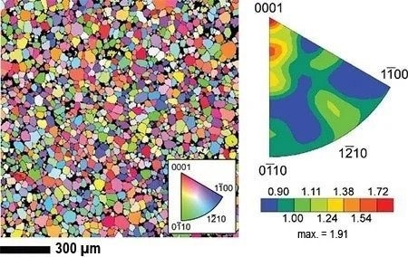
Orientation map and corresponding texture for a hot-pressed Al2O3 sample.
Image Credit:Gatan, Inc.
Can you explain how EBSD is adapted for TEM samples and the benefits it offers?
When working with TEM samples, especially those with nanoscale thickness, the challenge lies in obtaining microstructural and crystallographic information with high spatial resolution. Transmission Kikuchi Diffraction (TKD) overcomes this challenge by utilizing the principles of EBSD in a specialized manner.
In TKD, the sample is tilted, usually around 30 degrees, in the opposite direction of conventional EBSD, allowing the collection of EBSD patterns through the bottom of the sample. This approach significantly enhances spatial resolution, making it well-suited for analyzing ultra-thin materials like thin films or TEM lamellae.
The critical advantage of TKD is that it allows researchers to investigate these nanoscale materials at a microstructural level, offering insights into grain boundaries, orientation mapping, and phase identification. While TEM offers atomic-scale information, TKD complements it by providing a broader understanding of the material's microstructure. This combination of techniques is invaluable in materials science, as it allows researchers to gain both atomic-level and microstructural insights, ultimately enhancing their understanding of the material's properties and behavior at these tiny scales.
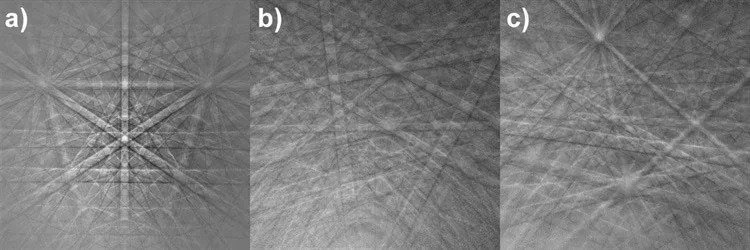
High-quality EBSD patterns collected with Clarity from a) silicon, b) olivine, and c) quartz.
Image Credit: Gatan, Inc.
In the context of phase identification, can you describe the extent of your phase identification database and its practical use for identifying unknown phases?
Our phase identification database, which includes approximately 500 common phases, is a valuable resource for researchers and scientists working with various materials. It allows us to identify known phases quickly and effectively within samples. This is particularly helpful when dealing with well-characterized materials and standard applications.
However, the database may have limitations when encountering materials that contain unusual or rare phases or in cases where researchers need more extensive and diverse phase information. Large online resources like the ICDD PDF 5+ database, which boasts a collection of over one million phases, come into play to address these scenarios. These comprehensive databases are a powerful tool for identifying unknown phases, mixtures, or complex materials, allowing researchers to delve deeper into the composition and structure of their samples.
The practical utility of these extensive databases is immense. When confronted with an unfamiliar phase or a complex mixture, scientists can use these databases to compare the collected diffraction patterns from their samples to those stored in the database.
This comparison leads to accurate phase identification, expediting the material characterization process. Furthermore, it provides insights into the material's properties and behavior. This is pivotal in various scientific disciplines, such as materials science, geology, and metallurgy, where understanding the composition and phases of materials is essential for research and development.
When a phase doesn’t have a good match in any of the phase databases, it can be difficult to determine what the material is. This is an ongoing topic of research within the EBSD community.
What are the temperature limits for conducting EBSD without damaging the detector, and what precautions should be taken for high-temperature EBSD?
EBSD does pose some unique challenges in-situ experiments in the SEM. The first is the high tilt required for obtaining high-quality EBSD patterns. While we generally aim for a 70-degree tilt for EBSD, this number is not set in stone. Some deviation can be tolerated and may be necessary when accommodating a heating or mechanical stage into the EBSD/SEM geometry.
The orientation map overlaid on an intensity map based on EBSD pattern quality on a hot-pressed MgAl2O4 sample.
Image Credit: Gatan, Inc.
Experimenting as quickly as possible is advisable to minimize drift, especially when using SEMs with less stable stages. This approach helps limit electron buildup on the sample surface and thus minimizes potential drift issues that can affect the quality of EBSD results. Furthermore, the emission of light from the sample due to the high temperature should also be considered. This light emission can impact the EBSD patterns and must be factored into the experiment setup. The EDAX Velocity detectors include an integrated IR filter to mitigate these effects.
A common question is how high a temperature can be achieved during in-situ experiments. The answer to this can be tricky and subtle. The energy radiated during heating is a function of the volume of the material being heated, so the smaller the sample, the less radiation. This, in turn, means it is easier to protect the EBSD detector and SEM when analyzing smaller samples. Our Velocity EBSD detectors have been used for phase transformation analysis in iron and titanium systems at temperatures over 1000 °C.
Maintaining a balance between high-temperature EBSD experiments and safeguards to protect the detector is crucial for obtaining accurate and reliable results.
Could you explain how carbon coating impacts EBSD analysis data and any alternative strategies for non-conductive samples?
Carbon coating is primarily employed to mitigate issues related to the poor conductivity of certain materials, such as ceramics or rocks. Coating the sample with a thin carbon layer helps enhance its electrical conductivity, thereby ensuring that the electrons can effectively return to ground instead of building up on the sample surface. The build-up of electrons can cause the beam to drift from the desired position, leading to distorted microstructure maps. Thus, even in conductive samples, it is important to connect the sample to ground to achieve distortion-free EBSD mapping (or any SEM-based imaging). It is important to ensure that the carbon coating is applied uniformly and thinly to avoid excessive scatter, which can affect the quality of the acquired EBSD patterns.
In EBSD analysis, it is not only about using carbon coating but also about being strategic in its application. One approach is using a mask over the sample, followed by applying carbon or gold coating over the entire sample. Afterward, the mask is removed, allowing researchers to focus solely on the region of interest. This method minimizes the potential drift and maximizes the data quality obtained from non-conductive samples.
It is important to note that while carbon coating is a widely adopted technique for addressing non-conductive samples, researchers are continually exploring alternative strategies and more advanced solutions to improve EBSD analysis for such materials. These efforts are part of the ongoing evolution of EBSD techniques and technologies, aiming to enhance their applicability across a broader range of material types and research requirements.
What are your insights on the future of EBSD? Are there potential developments and emerging areas of application that you find promising?
The future of EBSD seems promising, driven by several key factors. The first is the ongoing technological advancement in both EBSD hardware and software. For instance, developing more advanced detectors, such as direct detectors, enables higher-quality pattern collection and efficient operation at lower beam doses, improving the accuracy and reliability of EBSD data. Additionally, automation and data analysis improvements have made EBSD more accessible, facilitating its adoption across various scientific disciplines and industries.
One particularly exciting area of development is 3D EBSD and serial sectioning. This approach allows researchers to reconstruct and analyze microstructures in three dimensions, providing insights into grain morphology, orientation relationships, and the behavior of defects. This is especially beneficial in materials science and geology, where understanding microstructural evolution is crucial.
There is a growing interest in using EBSD to characterize complex and challenging materials. The ability to investigate organic and biological samples opens up new possibilities, ranging from studying tissues to understanding biomaterials' behavior, which could have profound implications in biology and medicine. In these applications, direct detection is a crucial advantage to avoid beam damage in these sensitive materials.
As the applications of EBSD expand, the technique is expected to contribute significantly to scientific and industrial advancements. Whether for developing new materials, quality control in manufacturing, or investigating geological processes, EBSD is poised to play a pivotal role in providing valuable microstructural insights that were previously challenging to obtain.
Dr. Stuart Wright
Stuart Wright was first introduced to EBSD as an undergraduate student at Brigham Young University, working with the first system in North America. He then moved on to Yale University to pursue a PhD under Professor Brent Adams. His thesis research focused on automating the EBSD technique. This effort led to the first fully automated EBSD scans in the fall of 1991. After graduating, Stuart joined Los Alamos National Lab and continued work in micro-texture and texture analysis using both the OIM technique and conventional x-ray diffraction. Shortly after TSL was founded, Stuart left Los Alamos and joined the startup company commercializing the OIM technique, working primarily on software development. He has continued in this role through the purchase of TSL by EDAX and then AMETEK. The original OIM system at Yale could index approximately one pattern in 3 seconds. Modern systems have come a long way since those early days, with speeds now exceeding 6,700 indexed patterns per second. Stuart is closely involved in the continued development of the technique, as well as in working with scientists all over the world in applying the technique to their materials research.

This information has been sourced, reviewed and adapted from materials provided by Gatan, Inc.
For more information on this source, please visit Gatan, Inc.
Disclaimer: The views expressed here are those of the interviewee and do not necessarily represent the views of AZoM.com Limited (T/A) AZoNetwork, the owner and operator of this website. This disclaimer forms part of the Terms and Conditions of use of this website.