Please can you introduce Bruker Optics and tell us about its FTIR-based solutions for the semiconductor industry?
Bruker Optics stands as the worldwide leader in FTIR spectroscopy, boasting over 60 years of experience. Since the explosive growth of the Silicon (Si) industry in the 1990s, Bruker has been at the forefront, providing tailored QC solutions. By maintaining active communication with leading Si manufacturers, Bruker remains attuned to industry trends, continually updating solutions to meet current demands.
In recent years, there has been a global boom in the silicon industry due to the increasing need for semiconductor devices in daily life. There is another driving force from geopolitical issues. In the past, the semiconductor industry had a well-established global supply chain. However, since the pandemic, industries have preferred to opt for more localized supply chains.
To address the complexities of this evolving landscape, it's imperative to have precise techniques for quality control (QC), research and development, and other critical processes.
Bruker delivers a diverse portfolio of FTIR-based solutions tailored to a myriad of analytical needs. This encompasses silicon applications across various conditions and parameters. Whether it is room temperature or low-temperature testing, analysis of thin wafers or entire silicon ingots, routine or highly sensitive examinations, customized quantification methods or standardized ASTM calibrations, or from laboratory-level to industrial automated operations—Bruker offers a solution.
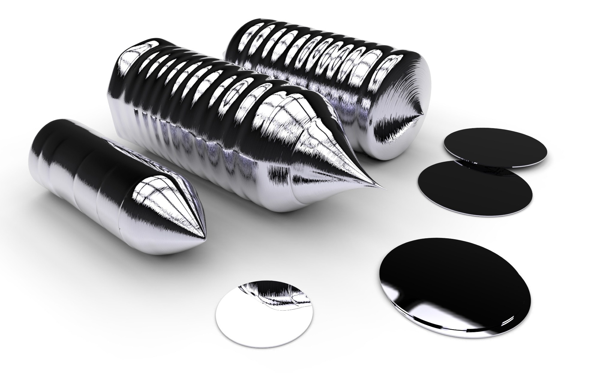
Image Credit: Adobe
What kind of information can FTIR provide for a silicon sample?
FTIR has been effectively used for QC in various silicon-based manufacturing processes. Its application is particularly prevalent in upstream manufacturing within the industry. For instance, it is employed in the assessment of photovoltaic wafers or ingots, as well as electronic-grade wafers or ingots. In these contexts, it is imperative to meticulously check the purity of wafers/ingots, either for categorization purposes or to fine-tune properties for subsequent research and development.
Si crystals, whether in the form of small pallets or wafers, can usually be analyzed using FTIR in transmission mode as well as photoluminescence mode.
With room temperature transmission measurements, it is possible to determine the concentrations of substitutional Carbon and interstitial Oxygen in Si, typically in the ppma range. For even greater sensitivity and a reduced detection limit, low-temperature transmission measurements can be employed, which can discern Carbon and Oxygen levels down to the ppba range.
At these lower temperatures, it is also feasible to detect shallow impurities like Boron (B), Phosphorous (P), Arsenic (As), Aluminium (Al), Gallium (Ga), Indium (In), and Antimony (Sb). The concentration of these group III and V impurities can be detected even at ppta levels.
For the highest-quality electronic grade Si samples, wherein the concentrations of B, P, Al, and Sb impurities are considerably lower by at least an order of magnitude, the photoluminescence (PL) method proves to be especially effective.
What are the difficulties of measuring Si ingots compared to wafers?
Ingots are broad, meaning that measuring ingots requires a high-performing FT-IR system with a high throughput and signal-to-noise ratio. Additionally, due to their weight, the at-line system should be equipped with an automated sample table designed to accommodate heavy samples.
How can FTIR be used in carbon and oxygen concentration analysis?
Carbon and oxygen concentration analysis is a very common application. Two ASTM standards are related to carbon and oxygen quantification in silicon crystals. Normally, you are asking for a detection limit of several hundred ppba. The FTIR technique fits this requirement perfectly. As long as the silicon crystal sample is high purity, you can use the FTIR technique to do such a quantification.
At Bruker, we offer the INVENIO and VERTEX spectrometers, which carry out quantification automatically.
Depending on the sample size, whether it is small single crystals or bigger wafers, we can put them onto different sample holders or wafer holders to do the measurement.
FTIR is suitable for quantification because carbon and oxygen in silicon crystals introduce specific molecular vibrations distinct from the inherent silicon phonon bands. By examining the absorption peaks associated with carbon and oxygen, it is possible to derive their concentrations. All these calculations, including the factors used, adhere to the ASTM standards.
For optimal results in this application, we recommend our INVENIO and VERTEX FTIR spectrometers. For a sample thickness of 1.5 millimeters, they can achieve an impressive detection limit of 200 ppba. Conversely, for wafer samples, which tend to be thinner than individual crystal samples, the detection limit ranges between 1-2 ppma.
Is there a more sensitive way to do concentration analysis?
The CryoSAS offers solutions with heightened sensitivity, primarily achieved by cooling down the system to enhance analytical sensitivity. While at room temperature, the detection limit for carbon might be several hundred ppba, cooling the system to 10 kelvin can significantly improve this. For instance, at this temperature, the detection limit for carbon drops to around 25 ppba and for oxygen to approximately 10 ppba.
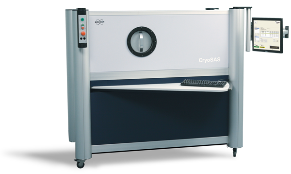
Image Credit: Bruker Optics
However, enhanced sensitivity is not the sole advantage of the CryoSAS. It is also adept at shallow impurity concentration analysis. The system is capable of detecting a wide range of elements, including carbon, phosphorus, boron, antimony, gallium, aluminum, indium, and antimony, and can measure these elements concurrently.
What kind of special setups are needed to achieve low-temperature conditions?
This technology deals with extremely low-temperature conditions between 4-15 kelvin.
In the past, users have had to deal with the liquid helium cryostat to achieve such low temperatures. However, operations with the cryostat and liquid helium are quite complicated and need experienced, hands-on skills. There is also a shortage of liquid helium resources, making it harder and more expensive to get in some parts of the world.
Cryogenic techniques have developed quickly in the last few decades, so more convenient methods are now available, such as close-cycle cryostat, where no cryogen is needed. The cooling process is also well programmed in the software so that the users can cool down the setup with one mouse click.
What advantages do Bruker’s photoluminescence (PL) modules have?
The FTIR solution combined with the PL setup offers convenience, simplicity, and speed. Using the PL system, you can achieve measurements for concentrations of elements that fall below the CryoSAS's detection threshold. Moreover, low-temperature photoluminescence provides a significantly lower detection limit compared to transmission methods such as the CryoSAS.
A notable advantage of our low-temperature PL system is the extensive detection range of our FTIR detector. This is particularly beneficial when different elements span varied wavelength ranges. Notably, our software is designed to automatically transition between these ranges.
Furthermore, our expertise in PL characterization extends to cutting-edge semiconductors, encompassing quantum dots, quantum wells, and type-II superlattices. We can conduct PL characterizations in the mid-infrared spectrum, covering wavelengths from 1-10 micrometers and even up to 16 micrometers with the vacuum PL module.
Understanding that many customers have unique requirements, we encourage direct communication. If you have specific PL needs, please reach out so we can assist you with the most fitting solution.
Besides impurity concentration determination, are there any other interesting questions that can be answered by FTIR techniques?
FTIR has a range of applications, with epilayer analysis emerging as one of the most prominent. The practice of depositing an epilayer on wafers is gaining traction, mainly to refine the wafer's electronic, optical, or physical attributes.
A key QC task post-deposition is to verify the thickness of the epilayer(s). This is where the reflectance mode of FTIR spectroscopy comes into play. By examining the interferences in the reflectance spectrum, which arise due to the layered structures, it is possible to determine the thickness of the epilayers.
At Bruker, we pride ourselves on offering advanced methods specifically tailored for epilayer structure analysis.
How efficient is the FTIR measurement for daily Si QC tasks?
FTIR is one of the fastest analytical tools available. Typically, routine tests are completed within a mere minute. The efficiency of FTIR is further elevated when equipped with autosamplers. While it might be beneficial to slightly extend the measurement time for enhanced sensitivity in certain exceptional cases, it remains comfortably within the minute range.
FTIR is fast, non-destructive and highly sensitive. The tool is also economical and easy to use when compared to other tools.
Why is it beneficial to be able to measure Si ingots?
In the past, direct measurement of ingots using FT-IR was not possible. Instead, ingots had to be sliced into wafers, and each wafer would then be individually assessed in a QC lab. These wafers, varying in purity, exhibit different electronic properties and thus needed to be categorized for subsequent stages of the Si manufacturing process.
Nowadays, the process is more streamlined, and it is possible to ascertain which part of an ingot is suitable for a specific manufacturing department even before slicing it. Once cut, there is no need to measure every single wafer. Instead, random checks suffice, significantly saving time and costs.
Take oxygen concentration in ingots, for instance. Traditionally, given that its concentration is not uniformly spread throughout an ingot, the entire ingot would be divided into thousands of pieces for individual analysis. This process necessitated thousands of measurements.
However, with advancements like the SiBrick Analyzer System (SBS), a preliminary check for oxygen can be conducted without slicing the ingot, offering substantial time savings for customers.
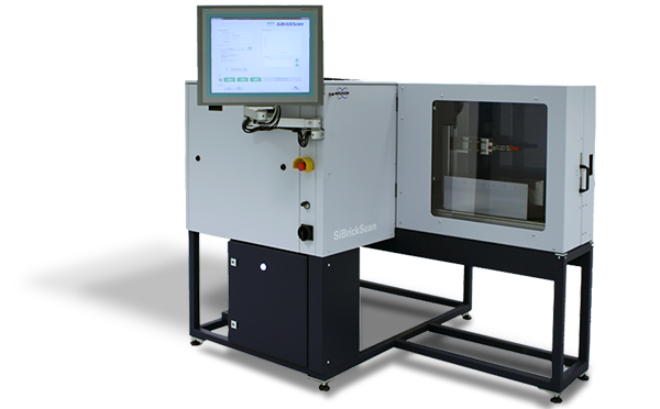
Image Credit: Bruker Optics
Are there any daily consumptions for the FT-IR systems?
No cryogenic cooling is required, and no one-way parts are necessary. Only cooling water and purge gas are consumed. Water can be used in a cooling cycle, and dried air can be used for purging.
Are there any internal standards for Si QC tasks based on the FTIR technique?
Yes. We usually refer to these four ATSM/SEMI standards: SEMI MF1391-0704, ASTM F1188-93, SEMI MF1630-0704, and SEMI MF1389-0704.
In these, the quantification/calibration methods and the FTIR spectroscopy conditions are clearly defined. As a Si QC solution provider, Bruker has implemented these standardized requirements in our systems.
Does the operation or handling of the FTIR instruments require well-trained personnel?
The FTIR design is user-friendly, meaning that a technician or chemical technical assistant can handle it with ease. The features include touchscreen control, one-click measurement start, and direct reports with no need to analyze IR spectra. All these features ensure simple operation and save personal costs.
About the speaker
Dr. Michael Jörger is Head of Business Unit Science at Bruker Optics, a division of Bruker Corporation.
This information has been sourced, reviewed and adapted from materials provided by Bruker Optics.
For more information on this source, please visit Bruker Optics.
Disclaimer: The views expressed here are those of the interviewee and do not necessarily represent the views of AZoM.com Limited (T/A) AZoNetwork, the owner and operator of this website. This disclaimer forms part of the Terms and Conditions of use of this website.