Analyzing failures in printed circuit boards (PCBs) is critical to ensure the functionality and reliability of electronic devices. A synopsis of the methods and techniques utilized in PCB failure analysis is presented here, starting with initial symptom identification and continuing through in-depth analysis using advanced spectroscopy and microscopy.
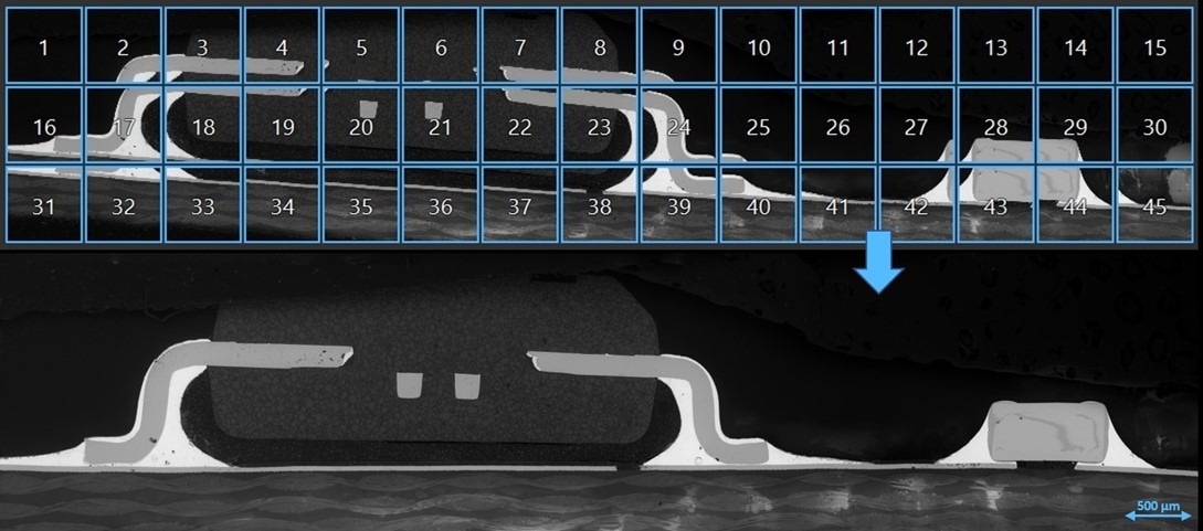
Figure 1. Acquisition and stitching of a sequence of 45 high-resolution BSE images using Coxem’s Panorama Mode. Image Credit: COXEM Co. Ltd
Discussed are the primary considerations in preparing samples, techniques for analysis, and often-seen failure mechanisms, highlighting the significance of quality control and the following of industry standards. In addition, advancements in scanning electron microscopy (SEM) technology are discussed, particularly using Panorama Mode in Coxem SEMs for complete fault localization and characterization.
Optical microscopy, FT-IR spectroscopy, and SEM-EDS analysis are used to examine the multidisciplinary approach needed for effective PCB failure analysis.
Introduction
Printed circuit boards are the keystone of contemporary electronic devices, supporting the functionality and interconnection of electronic components. However, even with rigorous quality control measures throughout production, PCBs can fail due to material defects, environmental contaminants, soldering issues, or mechanical stress.
Accurately diagnosing and resolving these failures is critical for maintaining the product's reliability and minimizing downtime. In this way, PCB failure analysis is pivotal and employs many combined analytical techniques to discover the root causes of failures.
Symptom Identification and Initial Examination
PCB failure analysis starts with identifying symptoms that indicate potential faults. These symptoms can manifest as anomalies, such as discoloration, contamination, suspicious solder joints, mechanical damage, or corrosion. Using a stereomicroscope in the initial examination enables a preliminary assessment of the PCB's condition and provides valuable insights into the nature and extent of the fault.
Sample Preparation
To arrive at a more detailed analysis, samples from the PCB are prepared with care taken to avoid introducing artifacts or damage. The samples must be cut precisely to prevent delicate materials from cracking, including glass or ceramics.
Mounting and lapping require caution to avoid mechanical fracture or deformation, especially in fragile components. The polishing process also requires careful attention to limit residues and ensure the surface is pristine for analysis, an essential step for accurate fault characterization. Ideally, these processes are performed using an ion mill, such as the Coxem CP-8000+.
Analytical Techniques
Various analytical techniques are used in PCB failure analysis, varying from optical microscopy to Fourier-transform infrared (FT-IR) spectroscopy. However, scanning electron microscopy with energy-dispersive X-Ray spectroscopy (SEM-EDS) is still the most comprehensive tool for characterizing the failure site, as it offers high-resolution imaging and elemental analysis capabilities. SEM-EDS allows for the evaluation of material chemistry, identification of failure mechanisms, and detection of external contaminants, providing comprehensive insights into the fault's nature and origin.
Common Failure Mechanisms
There are two technologies for mounting components on the printed circuit: the traditional through-hole technology (THT) and the newer surface mount technology (SMT) technique.
A spectrum of issues commonly cause PCB failures, ranging from component failures to solder defects and mechanical stress-related phenomena. Included are microcracks, solder layer cracks, corroded holes, cold solders, defective or shorted pads, flux residues, electromigration, thermal fatigue, and mechanical overload.
Understanding these failure mechanisms is crucial for targeted analysis and effective mitigation strategies.
Advanced SEM Techniques
Innovations in SEM technology, such as the Panorama Mode available in Coxem SEMs, provide improved capabilities for fault localization and characterization (Figure 1).
With the capture of a sequence of images stitched together, Panorama Mode allows for creating high-resolution images that cover the whole area of interest. This functionality, paired with contrast enhancement offered by backscattered electron imaging, supports quickly identifying fault regions, and a detailed examination of microstructural features. Advanced features in EDS microanalysis software also allow precise characterization of material contamination and chemistry, contributing to a deep understanding of the fault's underlying causes (Figure 2).
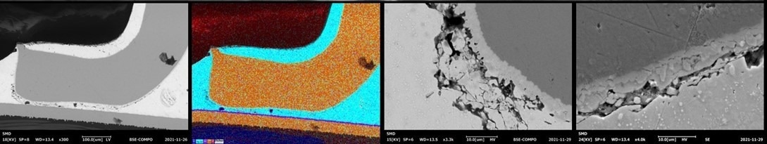
Figure 2. (left) BSE image and EDS map of solder of an SMD component. (right) Cracks in the solder layer and in the intermetallic phase visible in SE and BSE images. Image Credit: COXEM Co. Ltd
Conclusion
Investigating PCB failures requires a multidisciplinary approach, using various analytical techniques and advanced microscopy tools.
Through exacting sample preparation, meticulous analysis, and compliance to industry standards, the root causes of failures can be accurately identified, allowing for informed decision-making and implementation of effective corrective measures. Continued advancements in SEM technology promise to enhance the capabilities of PCB failure analysis and ensure the reliability and performance of electronic devices.

This information has been sourced, reviewed and adapted from materials provided by COXEM Co. Ltd.
For more information on this source, please visit COXEM Co. Ltd.