Sponsored by VeecoMar 12 2006
Initially introduced as an accessory to scanning tunneling microscopy (STM), atomic force microscopy (AFM) has become an advanced and most valuable scanning probe technique broadly used in academic and industrial research. A superior feature of AFM — the high-resolution visualization of surfaces — defines most of its applications. On one hand, AFM microscopes are employed for imaging of individual molecules and manipulations of nanometer-scale objects. On the other hand, they are widely applied for quality control in a number of industries where AFM is used for measurements of surface roughness and for quantitative examination of shapes/profiles of technologically important surface structures, such as DVD and CD patterns.
Over the past decade, many researchers working with soft matter (biological objects and polymers) have recognized the importance of this method. Nanometer-scale features as small as individual macromolecules, their assemblies, and larger-scale morphologies, can be easily recognized in AFM images. In addition, the fact that the stiffness of AFM probes is comparable to the stiffness of polymer materials makes it possible to distinguish sample locations with different mechanical properties. In this way, various components of heterogeneous polymer materials can be identified in the images.
For many years, examination of polymer samples with AFM was performed at ambient conditions and under liquids. These studies have been recently extended to different temperatures. In this manner, AFM can be used for in-situ monitoring of structural changes induced by thermal transitions, and for visualization of structure transformations caused by swelling and other effects. This application note presents several novel AFM applications to polymers.
Optimization of AFM Experiments
Compared to other microscopic techniques, AFM is still in its infancy. The capabilities of AFM, especially in studies of soft materials, are continuously expanding with the ongoing development of instrumentation and the increasing practical experience of researchers. Recent instrumental developments include a design of more precise actuators and more sensitive detectors, new operation modes, and specialized probes. There is also room for further improvement of overall microscope design and, particularly, lowering its thermal drift.
In practical AFM applications, it is well established that the tapping mode imaging technique is preferable to the contact mode technique. Depending on imaging needs, the experimental conditions should be adjusted either for high resolution and gentle profiling of surface features or for high-contrast visualization of different components of heterogeneous polymer systems (polymer blends, block copolymers, polymer composites). In tapping mode, the level of the tip-sample force interactions is varied by changing the amplitude of free-oscillating probe (A0) and set-point amplitude (Asp), as well as by using probes with different stiffness. For example, low-force imaging (light tapping) is achieved by applying soft probes (stiffness as low as 0.3 N/m), using small A0 and Asp close to A0. These conditions are favorable for non-destructive, high-resolution imaging of soft materials.
A good criterion of light tapping is imaging, at which the phase of the interacting probe is close to its phase in free oscillation. An operation at elevated tip-sample forces, which can be achieved by lowering Asp, increasing A0, and by using stiff probes, is optimal for compositional imaging of individual components in heterogeneous materials. In many cases, individual components are distinguished by different contrast in phase images. For compositional imaging of multicomponent materials with rubbery components, the most pronounced phase contrast is usually achieved at hard tapping conditions (A0 = 80-100nm, Asp = 40-50nm, probes with ~40 N/m stiffness). In hard tapping of polymer samples with rubbery top layers, the tip depresses the samples and even penetrates into them thus it probes sub-surface structures. The tip penetration can reach hundreds of nanometers when imaging of rubber samples is performed with A0 higher than 100nm and Asp as small as 5nm.
High-Resolution Imaging of Polymer Structures
At present, the question of AFM ultimate resolution is still an open one. Since the beginning, AFM images obtained in contact mode have revealed crystallographic lattices of surfaces of organic and inorganic compounds but were unable to show isolated molecular scale defects (true molecular resolution). The use of oscillatory AFM mode in UHV allowed imaging with true atomic resolution on a number of crystalline surfaces, and even sub-angstrom imaging was achieved. Until recently, true molecular resolution in tapping mode in air was problematic. The use of novel ultra-sharp probes and an AFM instrument with low thermal drift makes this possible.
The example of tapping mode imaging with true molecular resolution, which was obtained in studies of polydiacetylene (PDA) crystal, is demonstrated in Figure 1. This polymer has a chemical structure presented by a sketch. The top surface (the bc plane) of its crystal is formed by terminal molecular segments of the chain side groups, which are packed in a rectangular cell with the main parameters: b = 0.491nm and c = 1.410nm. This image of PDA crystal shows not only the regular lattice, which is consistent with the crystallographic structure of the bc surface, but also a molecular-size defect. The image was obtained with an ultra-sharp probe, which is prepared by a plasma-assisted deposition of carbon spikes on the apex of a Si etched probe. The value of this probe is manifested not only on surfaces with an expected molecular- or atomic scale order but also in high-resolution imaging of less-ordered surfaces with corrugations and pores in the nanometer scale. The TEM micrographs of this probe, a routinely used Si etched probe, and a novel diamond probe are collected in Figures 2a-c. Such probes with sub-10nm apex size are invaluable for molecular-scale imaging.
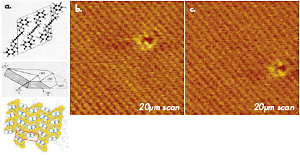
Figure 1. (a) A sketch of chemical structure, a crystal shape and crystallographic order at the bc plane for polydiacetylene (PDA) used for high-resolution AFM imaging. (b)-(c) Height images of the bc surface of PDA crystal obtained in tapping mode in air. Carbon spike probe is used in the experiments. The images show an ordered packing of surface groups and one molecular-scale defect. The images were recorded at the same location within a 10 min. interval. The shift of the defect is related to thermal drift of ~0.6nm/min.
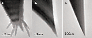
Figure 2. TEM micrographs of AFM probes. (a) Carbon spikes grown at the apex of Si etched probe; (b) Etched Si probe; (c) Diamond tip. TEM micrographs and diamond tip – courtesy of B. Mesa (MicroStar Technology).
A presence of a number of spikes at the extremity of the probes (Figure 2a) imposes definite restrictions on their use. Relatively flat samples should be studied with such probes to avoid the simultaneous interactions of the multiple spikes with the sample surface. The fragile nature of sharp spikes also requires gentle engage and imaging procedures. These prerequisites are less demanding in the case of Si etched probes and diamond probes, whose apex dimensions can be in the sub-10nm range.
Besides the use of sharp probes, an AFM microscope with low thermal drift (below 0.5nm/min) is important for molecular-scale imaging in tapping mode because of the slow scanning inherent to this method. With this lowthermal-drift instrument, molecular-scale resolution was also achieved in images of an oriented polytetrafluoroethylene (PTFE) layer and liquid crystalline material using a regular Si etched probe (Figure 2b) and a diamond probe (Figure 2c). The high-resolution images of PTFE are shown in Figures 3a-b. Flat crystalline terraces with steps of 0.56nm in height are seen at the surface of this layer (Figure 3a), which was prepared by hot rubbing on a glass substrate.
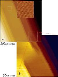
Figure 3. (a) Height image of PTFE layer obtained in tapping mode in air. Higher magnification images shown in the top part of Figures 3a-b were obtained at the locations marked with dotted lines. Etched Si probe was used in the experiments.
This indicates that the surface is formed of single molecular sheets. A high resolution image of the 10-nm location (top, left) shows individual polymer chains with 0.56-nm spacing. There are also a number of defects, some of which are magnified in Figure 3b. The dislocation defects marked by the circles are made of PTFE chains, which extend from one molecular sheet to another. One more example of molecular-scale imaging is presented in Figure 4, in which images of an annealed layer of star-shaped molecules on Si substrate are collected. The morphology pattern, which is seen in the large-scale image in Figure 4a, is common for liquid crystalline materials. On flat domains, one can distinguish a crystalline order with the almost orthogonal lattice, which is characterized by the repeat distances of 3.4nm and 3.6nm. A comparison of the AFM images with the results of X-ray analysis will help reveal the molecular packing in this layer.
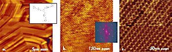
Figure 4. (a)-(c) Height images obtained on surface of liquid crystalline material in tapping mode in air. A sketch of chemical structure of disk-shaped star molecules forming this material is shown in the insert in (a). 2D FFT power spectrum of the image in (b) is shown in the insert. A lower half of the image in (c) is shown after filtering. Etched Si probe was used in the experiments.
Microscopic and nanoscopic objects are recognized in images by more than their specific shapes and dimensions. Visualization of single macromolecules, which adopt different molecular conformations depending on a deposition procedure and specifics of their interactions with a substrate, is one of the most exciting AFM features. AFM studies of DNA macromolecules, for example, became the routine procedure more than 10 years ago. Imaging at different tip-forces often leads to image-contrast variations that reflect local mechanical properties, and this procedure can be applied to single macromolecules. When imaging of DNA macromolecules (Figures 5b-c) placed on mica is performed at different forces, the contrast of the structure representing the macromolecule emphasizes either its overall shape or a more rigid core, which has lateral dimensions more closely corresponding to the expected size of DNA.
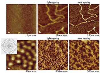
Figure 5. (a)-(c) Height images of DNA macromolecules on mica. Images in (b) and (c) were obtained at the same location at different tip-forces. (d) – (f) Height images of macromolecules of liquid crystalline carbosilane dendrimer on Si substrate. A sketch of the chemical structure of these molecules is shown in the insert in (d). Images in (e) and (f) were obtained at the same location at different tip-forces.
In another example (Figures 5d-f), spheres 5nm in size represent individual macromolecules of carbosilane dendrimer, which were deposited on Si substrate. Imaging of the aggregates of these macromolecules at different forces shows that the exterior of the macromolecules changes its contrast from bright to dark as the tip-force increases, Figures 5e-f. At the same conditions, the core of the macromolecules remains bright, which indicates its higher stiffness compared to the periphery of the molecules. This result corresponds to the higher density of the central portion of the molecules, which was confirmed by molecular dynamics simulations. In both cases, the image changes induced by tip-force are reversible and reflect variations of local mechanical properties. A use of AFM for studies of individual synthetic polymer molecules was first demonstrated by visualization of single chains of poly(styrene)-b-poly(methylmethacrylate) block copolymer and by monitoring changes of their conformation caused by humidity variations. This work was followed by a rapidly increasing number of applications in which single dendrimer molecules, macromolecular brushes, and polymers with mini-dendritic groups were observed with AFM. For such studies, single macromolecules are typically deposited on selected substrates (mica, silicon wafer, glass, graphite, etc.) from very dilute solutions.
The choice of substrate is essential for fixing macromolecules and unravelling polymer chains. The unraveling might be assisted by epitaxy of terminal alkyl groups to graphite, as it has been shown in studies of alkanes and polymer molecules with mini-dendritic side groups.
Imaging of single macromolecules is not a trivial procedure and one can expect difficulties in deducing the correct size of individual macromolecules from AFM images. While imaging isolated nanometer-scale objects on a substrate, it is rather hard to avoid a convolution of the tip shape with the shape of a macromolecule, as well as a possible tip-induced deformation of single macromolecules. These effects should be taken into account during analysis of the width and height of the isolated extended chain from the AFM images, yet the overall shape appearance and contour length of these macromolecules are reproduced in the images more correctly. Therefore, the images can be used for evaluation of the macromolecule conformation on different substrates and for construction of molecular length histograms, which provide direct information about molecular weight distribution.
An example of how AFM can be applied for conformation analysis of macromolecules on different substrates and in bulk was obtained in studies of macromolecules of polyphenylacetylene with mini-dendritic groups (Figure 6a).
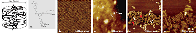
Figure 6. (a) Chemical structure of polyphenylacetylene with mini-dendritic groups and a sketch of the appearance of these molecules in bulk based on the X-ray analysis. Height images of these macromolecules on the fracture surface of the bulk polymer sample (b), in a single molecules domain on mica (c) and on graphite (d) and (e). The number in the insert of (c) indicates a length of four molecules marked with a white line in the image. The red arrows in the image in (d) show one of the molecular stacks on graphite.
In bulk, these macromolecules are arranged in a hexagonal lattice and the diameter of individual chains, which are formed by the core wrapped in a “jacket” of mini-dendritic groups, is around 5nm (X-ray data). The ordered chain layers, which were observed with AFM on the fracture surface of a bulk sample, exhibit a step height (4.5nm) equal to the macromolecule’s diameter. A spacing of 4.9nm was found
between the single chains seen in the image of a top surface of this sample (Figure 6b). These dimensions are close to the chain diameter (5.0nm) determined with the X-ray analysis.
The AFM images of the polymer chains on mica and graphite are shown in Figures 6c-d. The chain spacing of ~4.5nm, which was determined from the image of the polymer aggregate on mica, is similar with that found in the molecular layers on the fracture surface. When the macromolecules were deposited on graphite, their epitaxy led to a chain alignment along the main crystallographic axes of the substrate, Figure 6d. The width of the macromolecules on graphite as measured in three different stacks (one of which is indicated by red arrows) in this image is larger (6.5–6.6nm) than on mica. The height of the macromolecules on graphite (~0.79nm) is also substantially reduced compared to that on mica and on the fracture surface. These observations suggest that the polymer chains are flattened on graphite but retain an almost cylindrical shape on mica.
Self-assembly of macromolecules on a substrate takes place as the concentration of their solution, which is used for the deposition, increases. Domains of packed macromolecules on substrates can be more easily observed in AFM because they can withstand the tip-force better than single macromolecules. The main questions that are raised from the analysis of AFM images of macromolecular self assemblies on different substrates concern the interplay of macromolecular interactions within the polymer layer and those between macromolecules and substrates. The latter typically influence macromolecular order in one or several layers lying immediately on the substrate. Intermolecular interactions within the layers can originate from different mesogen groups and might dominate in polymer material with no relevance to the layer proximity to the substrate.
Several interesting results were obtained in AFM studies of alkane and polyethylene (PE) layers on graphite. What is seen in AFM images of alkanes is an alternation of the strips with different contrast either in height or phase images. The AFM images of C18H38, C36H74, and C60H122 alkanes in Figures 7a-c demonstrate that the width of the strips coincides with the length of the polymer chains. So far, AFM images showing individual alkane chains are not known, whereas visualization of individual –CH2- groups is usually achieved in STM images of alkane layers at the liquid-solid interface with graphite. In AFM images, arrays of the end –CH3 groups at the lamellar edges are typically seen as darker lines. This assignment is confirmed by imaging of C390H782 layers (Figures 8a-d) where the reversible variations in the height and phase images were observed as the tip-sample force interactions were varied.
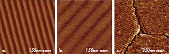
Figure 7. (a)-(c) Phase images of C18H38, C36H74 and C60H122 alkane layers on graphite.
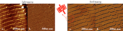
Figure 8. (a)-(b) Height (left) and phase (right) images of ultra long alkane C390H782 on graphite obtained in light tapping. (c)-(d) Height (left) and phase (right) images of the same location as in (a) and (b) obtained in hard tapping. All images were obtained at T=130°C. One of the local defects related to the alkane molecules forming a bridge between neighbouring lamellar ribbons is indicated with a circle in (c).
In light tapping, the height image represents the surface topography; therefore, the sites of –CH3 end groups of the alkane, which are bulkier than –CH2- groups, are seen elevated. A negligible contrast of the corresponding phase image confirms low tip-sample force interactions. When the tip-force increases (hard tapping), a possible tip deformation of regions of more mobile –CH3 groups makes these locations appear darker in height and phase images; thus, the images represent lamellar order of the alkane layers on graphite and help visualize various defects. One such defect, which is related to alkane molecules forming a bridge between neighbouring lamellar ribbons, is pointed out in Figure 8d.
Studies of polymer samples at elevated temperatures can yield invaluable information concerning the organization of adsorbate layers on different substrates. Particularly, our work on high-temperature imaging of layers of alkanes of different lengths (from C18H38 to C390H782) and polyethylene (PE) on graphite has shown that the order at the melt-substrate interface is retained at temperatures substantially exceeding the melting temperatures of the related crystals. In such measurements, the tip penetrates through a melt and reaches the lamellar layer lying immediately on the substrate. The structural rearrangement proceeds at high temperatures in the fashion shown by images of C390H782 alkane and PE in Figures 9a–f.
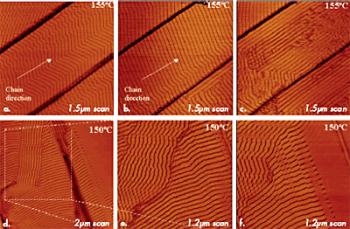
Figure 9. (a) – (c) Height images of ultra long C390H782 layers on graphite at 155°C. (d) – (f) Height images of polyethylene layers on graphite at 150°C.
In the case of the C390H782 layer (Figures 9a–c), after the temperature reached 155°C, zigzag-shaped lamellae of the middle terrace first changed to a straighter shape and then reoriented along the terrace edges. These alternations reflect the interplay of several interactions between the molecules within the layer and between the alkane molecules and the substrate. More bulky –CH3 end groups enforce the sliding of chains with respect to each other that caused the zigzag shape of the lamellae. With the temperature increase, molecular mobility was enhanced and enough space become available for the end groups of the neighbouring chains. This might explain the straightening of the lamellae. The increased molecular mobility also provoked a loss of registry of the alkane chains with one of the main directions of the graphite. As a result, the lamellar ribbons align preferentially along the terrace edges.
In the case of the PE layer (Figures 9d–f), the lamellar domains, which exhibited a well-defined orientation along the principal axes of the substrate (left image), gradually lost this epitaxial arrangement due to further increased molecular mobility (middle and right images). Ongoing isotropization of material, a loss of the lamellar order (see the right top corner of the right image), and breakage of individual lamellae into blocks is the result of local chain motion followed in this process.
Mapping of Multicomponent Polymer Materials
Multicomponent polymer materials are widely used in many industries because by appropriate mixing of different polymers and fillers one can design materials with desirable properties. The structure-property relationship in such materials is difficult to understand without microscopic analysis. AFM is very helpful in this analysis at scales from hundreds of microns to nanometers. The specific shape of individual components as well as variations in their mechanical and electric properties allow them to be distinguished from one another in AFMM images.
The images of two nanocomposites, polyparaxylylene with Si particles and polypropylene with clay, are shown in Figures 10a–b. Si particles, which are seen as small spheres with radii varying in the 5–10nm range, are dispersed in the polymer matrix. Small sheets of layered clay mineral, some of them in aggregates, are seen as edge-on structures in several locations in Figure 10b. The presence of aggregates indicates that the exfoliation process, which could separate the filler into multiple sheets with thickness down to molecular size, was not optimized.
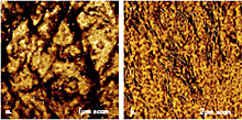
Figure 10. Phase images of polyparaxylylene filled with Ag particles (a) and polypropylene filled with clay particles (b).
Further efforts towards high-resolution observations of the individual nanoparticles in the sub-100-nm images will be quite desirable not only for visualizing their distribution in the matrix but also for determining specific shapes of nanoparticles in multicomponent materials and their proper assignment, which is rather difficult now.
Visualization of the microphase separated morphology (spherical, cylindrical, lamellar, or micellar) of block copolymers, which is characterized by structural parameters in the 5–50nm range, is one of the routine procedures in AFM applications. Domains of different components, which are formed as the result of phase separation of polymer blends, are typically of a larger size. AFM provides real-space observation of different coarsening processes and allows direct quantification of phase volume fractions and computation of domain interface curvatures of various morphologies. The contrast variations in AFM images of block copolymers and polymer blends are related to differences in the mechanical properties of the component. AFM allows studies of local mechanical properties at scales down to sub-micron by examining force curves in different sample locations.
The images in Figure 11 show that macroscopic testing of polymer properties could be extended to the nanoscale, which is important for developments in nanotechnology. The force curves present deflection-versus distance (DvZ) or amplitude versus distance (AvZ) dependencies. In applications for soft materials, DvZ curves are often recorded while the tip penetrates a sample and actually damages the surface layer.
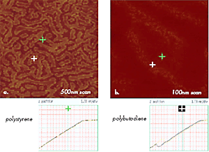
Figure 11. (a) –(b) Force Volume maps of 500nm and 100nm areas of polystyrene-b-polybutadiene-b-polystyrene film showing surface locations with different mechanical properties. Brighter areas as one marked with a green cross are characterized by AvZ curve shown below (a) and common for polystyrene; darker areas as one marked with a blue cross – by AvZ curve shown below (b) and common for polybutadiene.
Measurements of AvZ curves, which are less destructive and are characterized by smaller tip-sample area, are more suitable for probing surface mechanical properties with unprecedented resolution of 1nm. This is demonstrated in Figures 11a–b by force volume maps, which are built of 128x128 arrays of AvZ curves collected on the surface of a thin film of polystyrene-block-polybutadiene-blockpolystyrene (SBS) triblock copolymer.
The curves representing the tip interactions with polystyrene and polybutadiene blocks are different (Figures 11a- b); the different contrasts in the maps reflect the variations in Z-travel needed to damp the amplitude of the interacting probe to a trigger level chosen by an operator. Such experiments allow precise identification of surface locations occupied by different blocks and offer experimental data for nanomechanical models for extracting quantitative data, which is a challenging problem currently under careful examination. In further expansion of nanomechanical characterization of polymers with AFM, it will be crucial to examine viscoelastic responses of different polymer systems in a broad frequency range and at various temperatures.
AFM studies of polymer materials can be performed not only at ambient temperatures but also at elevated temperatures, as shown in the examples above (Figures 8–9). Recently, studies were expanded towards low temperatures: an example of imaging of a multicomponent polymer material is presented in Figures 12a–c. These images were obtained on a sample of roofing material at different temperatures. The contrast of the phase image at T = -10ºC differentiates a presumably rubber matrix and harder domains of another polymer, which have specific morphologies. The phase contrast has vanished at T = -35ºC, yet the domains became visible in the height image, most likely, due to differences in thermal contraction of the components.
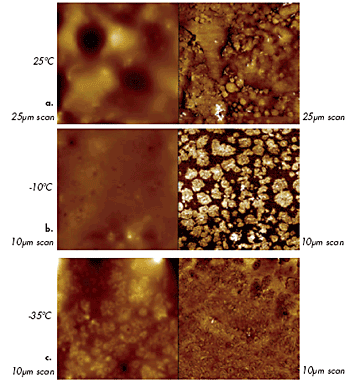
Figure 12. Height (left) and phase (right) images of roofing material at different temperatures: (a) 25°C, (b) (-10°C) and (c) (-35°C).
The variations in mechanical properties of different components of the roofing material with temperature are reflected in these images. This helps characterize the sample morphology. An earlier study, which was performed on a series of block copolymers, demonstrated that differentiation of the components of a heterogeneous polymer material is best achieved when imaging is conducted at temperatures above the glass transition (Tg) of one component and below Tg of the other component.
With the increasing penetration of polymer materials into the semiconductor, data storage, and flat panel industries, the examination of conducting and semiconducting properties of these materials at small scales is becoming an important research area. The capabilities of AFM-related techniques such as electric force microscopy (EFM), surface potential microscopy, and conducting and tunneling AFM have yet to be fully explored. As an application example of these methods we consider the images of a polymer blends filled with carbon black (CB) – thermoplastic vulcanizate, which are shown in Figures 13a-c. The sample for this study was prepared with a cryo-ultramicrotome. The height image in Figure 13a reveals the surface topography of one of the sample locations. A large number of bright particles most likely present the CB particles, which are distributed all over the sample. The EFM phase image in Figure 13b was obtained at the same location when the scanning probe was scanning slightly above the sample surface. The darker spots in this image indicate the conducting regions filled with CB, which contribute to a percolation network responsible for the conductivity of this sample. The CB particles, which are recognizable by their dimensions (40–60nm), are not limited to the dark regions. This means that merely a portion of the embedded particles contributes to the percolation network.
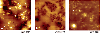
Figure 13. (a) Height image of thermoplastic vulcanizate obtained in tapping mode. (b) Phase image of the same location as in (a) obtained in electric force microscopy mode with a probe lift of 20nm. (c) Surface potential image of the same location as in (a).
The image in Figure 13c shows the distribution of surface potential at the same surface location. Bright spots (in the left side of the image) can be assigned to surface changes. Each of the images provides complementary information that can be invaluable in the characterization of electric properties of materials and their correlation with morphology and structure.
.png)
This information has been sourced, reviewed and adapted from materials provided by Veeco.
For more information on this source, please visit Veeco.