Introduction Doped CdS thin films are important for the fabrication of gas sensors and photovoltaic devices [1-3]. Indium is the one of the more effective dopants to obtain n-doped CdS because the extra electron coming from the In3+ ion is placed substitutionally in Cd2+ sites. During the past few years CdS:In thin films have been prepared by thermal evaporation [4], spray pyrolysis [5], chemical bath (CB) [6], and chemical bath plus indium diffusion [7] with good results. The most used technique to grow CdS for photovoltaic solar cells fabrication is CB [1]. In this way, it is important to develop an effective technique to n-dope CdS thin films during the growth process. Lokhande and co-workers reported the preparation of CdS:In thin films by CB, but with an amorphous structure [6], which represents a disadvantage for high efficiency solar cells design. In this work our principal concern is to increase the carrier density to reduce the electrical resistivity of the material, with no sensitive reduction of the forbidden energy band gap (Eg). In order to achieve this goal we employed the CB technique, in such a way that the aqueous solution containing Cd2+, In3+ and S2- ions, allows the formation of CdS:In. The doping method is analyzed for different impurity levels to determine the most effective dosage with good physical properties useful for a wide field of applications. Experimental The growth of polycrystalline CdS:In films was performed at 80 ± 1°C on glass substrates. Details of the CdS growth process have been previously reported in Ref. 8. Salt reagents (concentrations) used in the CdS:In preparation were: CdCl2 (0.02 M), KOH (0.15 M), NH4NO3 (1.5 M), SC(NH2)2 (0.2 M) and In(NO3)3-5H2O (0.1 M). The total solution (100 ml) for growing CdS was completed with relative volumes (Vr) of In(NO3)3.5H2O in aqueous solution, Vr ranging from 1.0 to 10.0 ml (1 ml = 1% Vr). This allowed us to study of the material with ten different doping In-levels. The samples are denoted as CdS:Inx, where x is the Vr value. The thickness of the layers was measured by a Dektak II profilometer, the X-ray diffraction (XRD) data were obtained using a Siemens D-5000 diffractometer with CuKα radiation. For the calculation of the (111) interplanar distance, the XRD peaks were fitted by using Lorentzian curves. In this way the center of each XRD peak was calculated up to ± 0.002 Å. The UV-Vis optical absorption spectra were recorded using a Unicam 8700 spectrophotometer. The shift Raman spectra were obtained with a Raman spectrometer with double grating SPEX model 14018. The photoconductivity was measured with a lock-in Stanford Research Systems Model SR530 and a monochromator ScienceTech Inc model 9490. Finally the carrier density was determined by measuring the Hall effect with a conventional apparatus from GMW Magnetic Systems model 3472-50. Results and Discussion XRD spectra of doped and undoped CdS thin films, with 300nm ± 10nm thickness, show the cubic zincblende (ZB) crystalline structure with a preferential orientation along the (111) direction [10]. The average (111) interplanar distance (d111) calculated from the XRD patterns of films from three different growth-series are displayed in Figure 1 as a function of Vr. For CdS:In1-CdS:In4 samples, d111 was, on average, smaller than the d111 corresponding to the undoped sample. This reduction only can be a consequence of the incorporation of In into the lattice. The smaller ionic radius of In3+ (0.94 Å) as compared with that of Cd2+ (1.02 Å) can be the cause for the decreasing of d111. Of course, this can only happen if In-ions enter substitutionally in Cd sites which occur in some other cation-doping-CdS cases. d111 in CdS:In5 to CdS:In7 is larger than in CdS:In0, we suppose in this case indium enters in both substitutionally and interstitially. For the CdS:In8 to CdS:In10 samples, d111 is again smaller than in the case of the CdS:In0 sample. Here, it is probable the indium impurities originate a lot of disorder in the CdS lattice in such a way that the lattice could be shrunken [9]. | 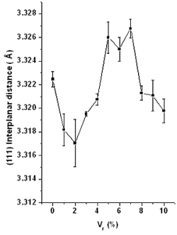
| | Figure 1. (111) interplanar distance calculated from XRD patterns versus Vr.differential thermal analysis curve (DTA). | The optical band gap (Eg ) values were obtained from optical absorption spectra by plotting (αhν)2 versus hν, where α is the optical absorption coefficient and hν the photon energy. From the photocurrent (IPC) spectra, Eg was also calculated by employing the plot (IPC.hν)2 versus hν [10]. Eg calculated by using these two methods is plotted in Figure 2a) against Vr for the different doping levels, the correspondence between the two methods to calculate Eg is very good. Figure 2b) illustrates the calculation of Eg for the CdS:In1 sample from the IPC spectra. The tendency of Eg as a function of Vr is, in general, a decreasing function, indicating the effects on the optical band gap of defects provoked by the introduction of In in the CdS volume. It is important to state that the percentage of the Eg decreasing is 2.1% when Vr = 10%. | 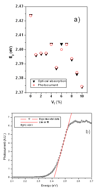
| | Figure 2. a) Optical band gap versus Vr determined from optical absorption spectra (triangles) and by photocurrent spectra (circles). b) Method for obtaining Eg by photocurrent spectra. | The characteristic LO phonon of the Raman spectrum CdS is observed centered at around 305 cm-1 in Figure 3 for the CdS:In3 sample. The band is asymmetric because the presence of the surface phonon band at lower frequencies, originated by the relative large ratio surface/volume in thin films [11,12]. The volume and surface contributions to the Raman band were deconvoluted using Lorentzian lineshapes as illustrated in Figure 3. In Figure 4 are displayed the center position for both bands for all the values of Vr. The trend observed by the experimental points in this figure indicates that for Vr ≤ 5% indium enters substitionally in the CdS lattice as this atom has larger atomic weight (114.82) than Cd (112.41), according to the larger mass, smaller in the frequency. For Vr > 5% this last statement in our case is not more valid probably because indium is also placed in interstitial positions. Indium in interstitial positions originates a different effect on the Raman frequency. | 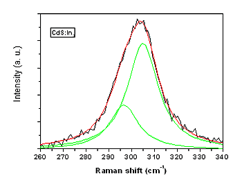
| | Figure 3. LO Raman band of CdS and deconvolution in two bands of the CdS:In3 sample. The lower energy band corresponds to the surface phonon, and the higher energy band to the volume phonon. | The majority carrier sign and density (n) of the doping as a function of the Vr was determined by Hall effect. As expected, the carriers are electrons, resulting in CdS n-type. The data are displayed in Figure 5 as a function of Vr. The carrier density increases approximately linearly up to Vr = 5%, then n diminishes with a large scattering of the experimental points, indicating a probable disorder in the lattice. The maximum density of the extrinsic carriers reach 4 x 1019 cm-3, reflecting an effective doping of CdS. The dark conductivity (σ) and the decreasing of the resistance in photoconductivity experiments (ΔR) are exhibited in Figure 6 as a function of Vr. Clearly, in both cases, the best result is obtained for Vr = 5%. The value σ = 10-1 Ω-1cm-1 can be considered a relatively high value for the conductivity for CdS:In thin films, doped during the growth process by CB. | 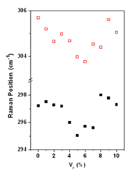
| | Figure 4. Position of the center of the Raman bands as a function of Vr. Volume phonon (top) and surface phonon (bottom). | | 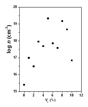
| | Figure 5. Carrier (n, electrons) density calculated form Hall effect measurements versus Vr. | | 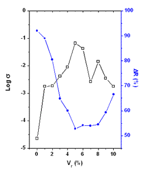
| | Figure 6. Dark conductivity (σ, circles) and percent photoresistance decreasing (ΔR) versus Vr | Conclusions We have successfully grown CdS:In thin films by chemical bath, the doping was carried out during the growth process by adding different relative volumes (Vr) of the aqueous solution containing In3+ ions. The experimental characterization indicates that for Vr = 5% the doping process is more efficient, obtaining an electronic density of 4 x 1019 cm-3 and a conductivity of 10-1 Ω-1cm-1, with decreasing in the optical band gap of only 0.85%. Acknowledgements The authors wish to thank Ing. A.B. Soto for her technical assistance. References 1. C. S. Ferekides, D. Marinskiy, V. Viswanathan, B. Tetaly, V. Palekis, P. Selvaraj and D. L. Morel, “High Efficiency CSS CdTe Solar Cells”, Thin Solid Films, 361/362 (2000) 520-526. 2. B. K. Maremadi, K. Colbow and Y. Harima, “A CdS photoconductivity gas sensor as an analytical tool for detection and analysis of hardous gases in the environment”, Rev. Sci. Instrum., 68 (1997) 3898-3903. 3. M. Kobayashi, K. Kitamura, H. Umeya, A. W. Jia, A. Yoshikawa, M. Shimotomai, Y. Kato and K. Takahashi, “Growth of CdS self-organized quantum dots by molecular beam epitaxy and application to light emiting diode structure”, J. Vac. Sci. Technol. B, 18 (2000) 1684-1687. 4. N. M. Megahid, M. M. Wakkad, E. K. H. Shokr and N. M. Abass, “Microstructure and electrical conductivity of In-doped CdS thin films”, Physica. B, 353 (2004) 150-163. 5. A. Palafox, G. Romero-Paredes, A. Maldonado, R. Asomoza, D. R. Acosta and J. Palacios-Gómez, Sol. En. Mater. & Sol. Cells, 55 (1998) 31-41. 6. R. S. Mane and C. D. Lockhande. ”Chemical deposition method for chalcogenide thin films”, Mater. Chem. Phys., 65 (2000) 1-31. 7. P. J. George, A. Sánchez, P. K. Nair and M. T. S. Nair, “Doping of chemically deposited intrinsic CdS thin films to n type by thermal diffusion of indium”, Appl. Phys. Lett., 66 (1995) 3624-3626. 8. J. L. Martínez, G. Martínez, G. Torres-Delgado, O. Guzmán del Ángel P, O. Zelaya-Ángel and R. Lozada-Morales, “Cubic CdS thin films studied by spectroscopic ellipsometry”, J. Mater. Sci. Mater. Electron., 8 (1997) 399-403. 9. E. Ustundag, B. Clausen and M. A. M. Burke, “Neutron diffraction study of the reduction of NiAl2O4”, Appl. Phys. Lett., 76 (2000) 894-896. 10. J. Kokaj and A. E. Rakhshani, “Photocurrent spectroscopy of solution-growth CdS films annealed in CdCl2 vapor”, J. Phys. D: Appl. Phys., 37 (2004) 1970-1975. 11. K. K. Nanda, S. N. Sarangi, S. N. Sahu, S. K. Deb and S. N. Behera, “Raman spectroscopy of CdS nanocrystalline semiconductors”, Physica. B, 262 (1999) 31-39. 12. A. Roy, A. K. Sood, “Surface and confined optical phonons in CdSxSe1-x nanoparticles in glass matrix”, Phys. Rev. B, 53 (1996) 12127-12132. Contact Details |