Direct write lithography is used in all phases of nanotechnology development activities. In research, it is utilized to create nanostructures into which functional materials can be patterned on the nano-scale. In process development, direct patterning allows the flexible creation of devices with varying features to optimize behavior. In manufacturing of semiconductors and data storage devices, direct write exposure with focused beams provides master patterns for processes such as photolithography and nano-imprint lithography.
Smaller Devices Pushes Demands on Lithography
The fabrication of ever smaller devices pushes the demands on lithography. Feature size and density are the two main considerations in this regime. Ion beam writing offers advantages in reduced proximity effects – allowing ideally for higher feature density, as is often defined by the lithographic half-pitch (half the distance between the most densely packed features). Ion beam writing also offers greater sensitivity. Traditional FIB, based on the liquid metal ion source, does not offer a small enough probe to make the smallest features and hence take advantage of its benefits. Electron beam writing can provide a smaller probe and thus has been the dominant technology for lithography.
Capabilities of The ORION PLUS Helium Ion Microscope for Direct Write Lithography
The helium ion microscope (HIM) provides a probe combining the small size available in electron beam systems with the favorable proximity effects of an ion. In fact, the nature of the beam-sample interactions for a helium ion is different from that of any other particle used for FIB, which should allow for even more localization in writing. Some HIM users have begun to do characterization of direct write lithography, and we will highlight some of the achievements here as an illustration of what can be done and also to point to the future research opportunities. The work described herein was carried out by Vadim Sidorkin and co-workers from the Delft University of Technology and from TNO Science and Industry in Delft, The Netherlands.
A lithography application requires two basic components. The first need is a thin film of material (resist) which will alter chemically when irradiated with the beam, becoming either resistant to dissolving during the development step (negative tone) or becoming more soluble (positive tone). The second need is a method to address the beam according to a pattern that is desired to be written. The ORION® PLUS offers two methods for accomplishing this. The system software offers the user an interface to set all the parameters that define an exposure. The total dose applied can be set using one of several measurement units, with the beam current being provided from the beam blanking unit in the ion column. The user defines a rectangular scanning area with arbitrary size and orientation. Either pixel density or spacing can be set within the box. The scanning pattern is also user selectable, with raster and serpentine scans in any orientation within the box. One can also acquire imaging signal during the operation. The scan parameters can also be saved as presets, for quick recollection and re-use. It is also possible within the user interface to import a bitmap with 256 gray levels to drive the scan. In this case, the relative dose at each pixel is defined by the gray level of the bitmap. For more complex patterns, or for more flexibility, the system is capable of being driven by an external pattern generator. There are several commercially available generators that offer advanced functionality and which have already been successfully implemented on the microscope.
For the work described here, initial characterization of resist behavior under helium ion writing was carried out. Hydrogen silsesquioxane (HSQ) resist films of thickness from 5 nm to 70 nm were prepared on silicon substrates. The first measurements were of resist sensitivity and contrast. This was carried out by exposing square areas under HIM with a 75 pA beam current, with the results displayed in Figure 1. This shows the normalized thickness remaining in this negative tone resist after development, as a function of dose. The resist became fully exposed at a dose 4.4 × less than for electron beam exposure, carried out in SEM. The contrast is similar for the two beams, so that the threshold between the "written" and "not written" states of the resist has equal performance in HIM.
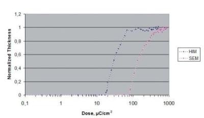
Figure 1. Response of HSQ under He+ and electron exposure.
The intriguing application result is the ability to write dense features. Figure 2 shows the result from writing an array of dots in 5 nm thick HSQ. A dot writing size of 6 nm ± 1 nm was achieved from a 1 pA beam at 100 µsec exposure time per dot. Most interesting is the fact that the dot size experienced no measurable proximity effect from the density of the array, even down to a half-pitch of 7 nm. This means that about 25 % of the area could be exposed with 6 nm resolution. To illustrate the throughput capability of this, a 10 µm × 10 µm area can be written with such pixel density in about 70 seconds. For thicker resist layers, the dot size does grow. Figure 3 shows 6 nm dots obtained in thin resist as compared to 14 nm dots in the thicker sample. The resist, however, is 10 × thicker in the latter case, so the aspect ratio of the features created grew from 1.3 to 3.9. This could offer a greater flexibility in 3D structuring.
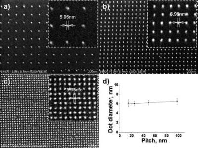
Figure 2. Dot exposures in HSQ. a) 48 nm pitch, b) 24 nm pitch, c) 14 nm pitch, d) plot of dot diameter vs. pitch.
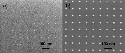
Figure 3. Dot exposures in HSQ. Left: 5 nm thick resist. Right: 55 nm thick resist.
Summary
We see in conclusion that lithography by HIM is a viable method that holds promise for high resolution, high density pattern creation. The tool also has the hardware and software features needed, including the external pattern generator interface, to write complex scans. We thank the TNO and TU Delft research groups at the Van Leeuwenhoek Laboratory, funded through the bsik NanoNed program of the Dutch Ministries of Education and Economic Affairs, for the permission to use their data and analyses here. Appreciation is also expressed to Raith GmbH who supplied the ELPHY Plus pattern generator used during the research.
Application
Direct write lithography in resists for creating high feature density structures with critical dimensions below ten nanometers. This is applicable in nanotechnology research, template fabrication, and device prototyping.

This information has been sourced, reviewed and adapted from materials provided by Carl Zeiss Microscopy GmbH.
For more information on this source, please visit Carl Zeiss Microscopy GmbH.