Advantages of Diamond Diamond exhibits a rare combination of physical, optical and thermal properties that make it an attractive material for many applications. It is the hardest material known to man, has the highest thermal conductivity at room temperature of any material, yet is electrically insulating and transparent from 225 nm through and beyond the IR region of the electromagnetic spectrum (except for a second order absorption at 5 μm). Some of diamond’s basic properties are listed in Table 1. Table 1. Properties of diamond compared to other selected materials. | | | Diamond | 2000 | 1 x 10¹⁴ | 110 | | Copper | 380 | 1.7 x 10⁻⁸ | 0.04 | | Alumina | 30 | 3.3 x 10⁸ | 20 | | Silicon | 168 | 3.2 x 10⁵ | 11.5 | | ZnSe | 140 | - | 1.7 | Disadvantages of Diamond However, those same excellent properties such as hardness and chemical inertness are a major disadvantage when it comes to processing diamond, and, as would be expected, it is expensive. Small, artificial, single crystal diamonds are produced, but this requires extremely high temperatures and pressures. Diamond grit is also produced commercially, and is used in the manufacture of cutting tools and for abrasive applications. Production of Diamond by Chemical Vapour Deposition (CVD) In the 1980s reports emerged from Russia suggesting that diamond could be formed from the vapour phase at relatively low temperatures and pressures. Although greeted at first with some scepticism, these reports generated a large amount of research into chemical vapour deposition (CVD) of polycrystalline diamond. Growth of Polycrystalline Diamond Polycrystalline diamond can be grown by a number of different CVD techniques, including microwave plasma assisted chemical vapour deposition, hot filament deposition, plasma jet deposition and combustion flame deposition. Microwave Plasma Assisted Chemical Vapour Deposition At GEC-Marconi Materials Technology, the microwave plasma assisted CVD technique is used for growing free-standing diamond, figure 1, typically between 50µm and 2000µm thick, and for growing coatings (<50μm thick), which can cover structures up to 200 mm in diameter. For self-supporting material the polycrystalline diamond is usually grown on silicon substrates, which are chemically removed after growth. The wafers can then be polished, processed and laser cut to the required device dimensions, figure 2. | 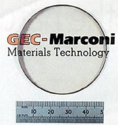
| | Figure 1. A 50mm diameter polished white diamond wafer. | | 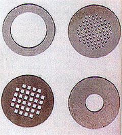
| | Figure 2. Diamond TEM grids (3mm in diameter). The high purity of the diamond and the low atomic number of carbon makes it an ideal substrate fro analytical purposes. | How the Deposition Processes Work All the deposition techniques rely on the ability to set up a dynamic non-equilibrium system, in which only sp3 carbon bonding can survive. This is achieved by the presence of hydrocarbon radicals, and more importantly, by large quantities of atomic hydrogen in the deposition gas. The hydrocarbon radicals provide the vapour source of carbon for diamond deposition. The atomic hydrogen is believed to play two important roles: it eliminates sp2 bonded carbon (graphite), while stabilising the dangling bonds of the tetrahedrally bonded carbon sp3. By creating a plasma system where atomic hydrogen predominates, any graphitic bonding is etched away, leaving only high quality diamond. Growth Rates and Grades of Polycrystalline Diamond The growth rate of polycrystalline diamond has a strong influence on the final quality of the material. Relatively high growth rates are possible, but at the expense of sample phase purity. This has resulted in the development of different grades of CVD diamond to cover the wide diversity of its applications. There are two main types. High quality, low growth rate white transparent diamond contains virtually no graphite, and is used in electrical and optical applications. High growth rate ‘black’ diamond, which contains small amounts of graphite, especially at the grain boundaries, is used for thermal management applications such as heat spreaders. Applications for Chemical Vapour Deposited Diamond CVD diamond is a relatively new material and many different applications for it are being investigated. However two areas in which it is already employed are cutting tool inserts and heat spreaders. Cutting Tools In cutting tool applications, the increase in hardness and heat dissipation offered over other materials allows tools to be operated at higher temperatures and for longer periods between renewal. This results in increased work through put and decreased downtime. Heat Spreaders Diamond has a thermal conductivity some five times that of copper at room temperature. This property, coupled with its high electrical resistivity, makes it an ideal material for use as heat spreaders for high powered electrical devices. Diamond heat spreaders are already used in the manufacture of solid state laser diodes. Semiconductors In the late 1980s it was (optimistically) suggested that diamond would be ‘the semiconductor material of the 21st century’. It exhibits a high band gap (~5.5 eV), excellent thermal conductivity, high breakdown field, high charge carrier mobility, negative electron affinity, high radiation tolerance and high sound velocity. However, it is difficult to dope because of the metastable nature of the diamond at normal pressures. P-type doping has been achieved using boron, but as yet there has been no successful n-type doping of diamond (although some promising work has recently been reported). Another difficulty is that diamond epitaxial layers have not yet been produced. When both epitaxial and n-type doped material become available, diamond will start to make inroads into the high power semiconductor market. The high cost of diamond will probably limit its use, but it will find applications in high value, specialist devices, where the improvement in performance outweighs the increase in cost. Electrical Devices Diamond could find applications in many different electrical devices, in doped or undoped form. These include FET and MOS transistor; negative electron affinity devices for use as electron field emitters, nuclear radiation detector and UV solar blind detectors. Microwave Communications One area where diamond is already being use is in surface acoustic wave (SAW) devices for microwave communications. The wavelength of an acoustic wave in a solid is 105 times shorter than that of an electromagnetic wave, so miniaturisation of microwave instruments is feasible. As with most electrical devices, there is a need for ever higher operating frequencies, and current materials (such as quartz and LiNbO3) are reaching their practical limits. The introduction of diamond will increase the possible wave velocities by three to four times that of current materials. Devices operating up to 2 GHz have already been demonstrated in Japan using CVD diamond. Solar Blind UV Sensors Since diamond is transparent in both the infrared and visible regions of the electromagnetic is spectrum, and exhibits a band gap at 5.5 eV (i.e. in the UV region), it is a candidate for use a true solar blind UV sensor. Such devices have already been demonstrated. Its transparency in the infrared region of the EM spectrum make it an ideal material for applications such IR windows and sensor heads. CO2 Laser Windows Diamond is hard, chemically inert and has a high thermal shock resistance, in contrast to many IR transparent materials such as ZnSe. One specific application for which it has great promise is as a CO2 laser output window. During operation, the window heats as it absorbs laser light, and this heat has to be dissipated to avoid distortion of the optical window. ZnSe is currently used as the window material, but it has a low thermal conductivity which limits the dissipation of this heat and therefore the operating power of the laser. Diamond’s excellent thermal conductivity dissipates heat better, so allowing higher power outputs. Other applications include IR sensor heads for use in chemically aggressive environments and as windows for airborne radars. RF and Microwave Devices Finally, diamond also has possible applications in RF and microwave devices. It is a possible replacement for sapphire in high power RF output windows and for alumina as a substrate material for microwave circuits. Again, its high thermal conductivity will result in increased power output. Summary As the cost of CVD diamond decreases, its use will increase and diversify further. However, as with any new material, two areas must be addressed if it is to become a commercially viable product. First, production costs must be reduced. This will be achieved not only by economy of scale as demand increases, but by the development of a new generation of deposition systems which will enable high quality diamond to be grown over ever larger areas. Secondly, new doping, processing and joining technologies need to be developed. This is not trivial, since the properties that make diamond attractive for so many applications (i.e. hardness, chemical inertness etc) also make it difficult to dope and process. Although diamond may not turn out to be the semiconductor material of the 21st century, it will play an important role in the electronic and microwave industries where the improvement in device performance will benefit us all. |