Nov 9 2016
Solar cells made of the highly popular and inexpensive perovskite material can use a new method to sandwich two forms of perovskites into one photovoltaic cell, and generate electricity from sunlight with increased efficiency.
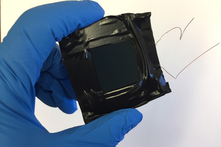 This first version of a new layered perovskite solar cell already achieves an efficiency of more than 20 percent, rivaling many commercial solar cells. Flexible and easy to make, it can produce more than half a volt of electricity. (Credit: Onur Ergen).
Much like the silicon-based solar cells today, perovskite-based solar cells are made of inorganic elements and organic molecules that work together to covert the captured light into electricity. However, perovskite photovoltaic systems can be produced more cheaply and easily than silicon-based cells, on a flexible instead of a rigid substrate. These perovskite-based solar cells have been reported to capture 20% of solar energy, and can be commercially available in 2017.
University of California, Berkeley, and Lawrence Berkeley National Laboratory scientists have reported a new design in a paper that has featured in Nature Materials on 7 November, 2016 prior to its publication. This design is capable of achieving 18.4% average steady-state efficiency, 21.7% high efficiency, and 26% peak efficiency.
We have set the record now for different parameters of perovskite solar cells, including the efficiency. The efficiency is higher than any other perovskite cell – 21.7 percent – which is a phenomenal number, considering we are at the beginning of optimizing this.
Alex Zettl, senior author, UC Berkeley professor of physics, senior faculty member at Berkeley Lab and member of the Kavli Energy Nanosciences Institute
“This has a great potential to be the cheapest photovoltaic on the market, plugging into any home solar system,” said Onur Ergen, the lead author of the paper and a UC Berkeley physics graduate student.
The efficiency is also higher than that of polycrystalline silicon solar cells, which have 10-20% efficiency and are used in most houses and electronic devices. The highest efficiency of the most purest silicon solar cells, which are extremely costly to produce, topped out at only 25% over 10 years ago.
The achievement was possible due to a new means of combining two types of perovskite solar cell materials, each made to absorb a different color or wavelength of sunlight, into a single “graded bandgap” solar cell that can absorb the whole spectrum of visible light. Attempts made in the past to combine two different perovskite materials have not been successful as each material degrades the electronic performance of the other.
“This is realizing a graded bandgap solar cell in a relatively easy-to-control and easy-to-manipulate system,” Zettl said. “The nice thing about this is that it combines two very valuable features – the graded bandgap, a known approach, with perovskite, a relatively new but known material with surprisingly high efficiencies – to get the best of both worlds.”
Full-Spectrum Solar Cells
Perovskite and silicon are semiconductors that can conduct electricity only when the sufficient energy is absorbed by electrons, for instance from a photon of light, to push them beyond a forbidden bandgap or energy gap. Such materials absorb light selectively at particular wavelengths or energies – the bandgap energy – but not sufficiently at other wavelengths.
In this case, we are swiping the entire solar spectrum from infrared through the entire visible spectrum. Our theoretical efficiency calculations should be much, much higher and easier to reach than for single-bandgap solar cells because we can maximize coverage of the solar spectrum.
Onur Ergen, the lead author of the paper and a UC Berkeley physics graduate student
A hexagonal boron nitride of single-atom thickness that resembles a layer of chicken wire was used to separate the perovskite layers, and proved to be the key to merging two materials into a single solar cell. The perovskite materials were made of the organic molecules ammonia and methyl; while one contained the metals iodine and tin, the other contained iodine and lead doped with bromine. The former layer is tuned to selectively absorb light with 1 electronic volt (eV) energy, and the latter layer is tuned to absorb photons with 2eV of energy, or amber color.
The boron nitride monolayer enables the perovskite materials to work in tandem, and produce electricity from across the entire range of colors between energy of 1 and 2 eV.
Zettl stated that the boron nitride/perovskite sandwich is deposited on top of a lightweight aerogel of graphene that operates as a moisture barrier, encourages the development of finer-grained perovskite crystals and helps in stabilizing charge transport through the cell. Perovskites fall apart due to moisture.
A gold electrode is used to cap the entire thing at the bottom, while a gallium nitride layer is used at the top to collect the electrons generated in the cell. The thickness of the active layer of thin-film solar cell is approximately 400nm.
Our architecture is a bit like building a quality automobile roadway. The graphene aerogel acts like the firm, crushed rock bottom layer or foundation, the two perovskite layers are like finer gravel and sand layers deposited on top of that, with the hexagonal boron nitride layer acting like a thin-sheet membrane between the gravel and sand that keeps the sand from diffusing into or mixing too much with the finer gravel. The gallium nitride layer serves as the top asphalt layer.
Alex Zettl, senior author, UC Berkeley professor of physics, senior faculty member at Berkeley Lab and member of the Kavli Energy Nanosciences Institute
More layers of perovskites, separated by hexagonal boron nitride, can be added; but, with the broad-spectrum efficiency of the cells, this may not be necessary, said the researchers.
“People have had this idea of easy-to-make, roll-to-roll photovoltaics, where you pull plastic off a roll, spray on the solar material, and roll it back up,” Zettl said. “With this new material, we are in the regime of roll-to-roll mass production; it’s really almost like spray painting.”
S. Matt Gilbert, Thang Pham, Sally Turner Mark and Tian Zhi Tan of UC Berkeley and Marcus Worsley of Lawrence Livermore National Laboratory, who created the graphene aerogel, are the co-authors of the study.
The National Science Foundation, the Office of Naval Research and the U.S. Department of Energy supported the research endeavor.