Over the past 10 years compound semiconductors have gained considerable attention since they exhibit characteristics ideal for next-generation devices.
Historically, material challenges have hampered the fabrication of these devices. Although these challenges have chiefly been overcome at the research level, difficulties still persist while moving to industrial production.
Renishaw’s inVia Raman microscope is a non-destructive, non-invasive characterization tool that offers spatial, sub-micrometer information on the electronic, crystal, and vibrational structure of materials. During the measurement of compound semiconductors, the system can be used to gather Raman and photoluminescence (PL) spectra enabling the following information to be acquired:
- Sample topography
- Alloy percentages
- Sample temperature (in operating devices)
- Strain/stress
- Dopant concentrations
- Contamination identification
- Thin film thickness
- Crystal structure type and orientation
- Particulate analysis, for example, SiC inclusion
- Chemical identification
- Crystal quality and defect levels
- Sample uniformity
This article provides a few examples to show the power of the inVia Raman microscope and its potential to analyze material challenges. These include the evaluation of heterostructures in GaN-based semiconductors and thermography.
Evaluation of AlGaN/GaN Heterostructures
For several years, the development of GaN-based devices was hampered by materials of low quality. High quality materials are now available, however the scale-up needed for mass production is still difficult, as is optimising the process and the equipment used.
This article illustrates the use of inVia Raman microscope as a quality control tool to analyze GaN based wafers. The analyzed wafer consists of a 30-nm Al0.28 GaN0.72 layer on a 2-µm GaN layer formed on a 300-µm sapphire substrate. PL and Raman spectra were obtained using distinctive laser excitation wavelengths, enabling distinctive layers in the structure to be analyzed.
The spectra obtained from the distinctive layers of the structure, at different excitation wavelengths, are shown in figure 1 and figure 2. Investigation of these modes enables quantification of aluminum content, free carrier concentration, stress and crystal quality.
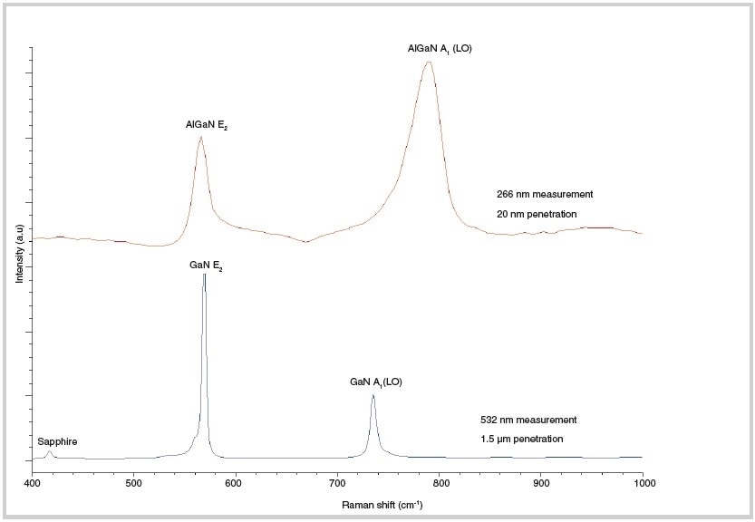
Figure 1. Raman spectra of different layers in a AlGaN/GaN heterostructure. The depth probed by Raman spectroscopy is dependent on the excitation wavelength. Here, a UV excitation laser is used, allowing the ultrathin AlGaN layer to be measured.
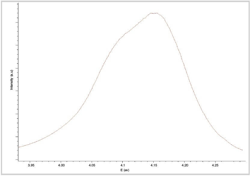
Figure 2. Photoluminescence (PL) spectrum of the AlGaN layer.
Here, investigation of the GaN layer shows a high level of uniformity with variations in stress, as illustrated in the E2 peak position in figure 3 (a).
It was found that the AlGaN layer had considerable variation in Al concentration at the edge of the wafer (up to 5 mm inward radius) of about 0.5%. One of the added advantages of the inVia Qontor Raman microscope is that the sample’s topography is measured at the same time as the Raman measurements, enabling the bow of the wafer to be ascertained. This is shown in figure 3 (b) and (c).
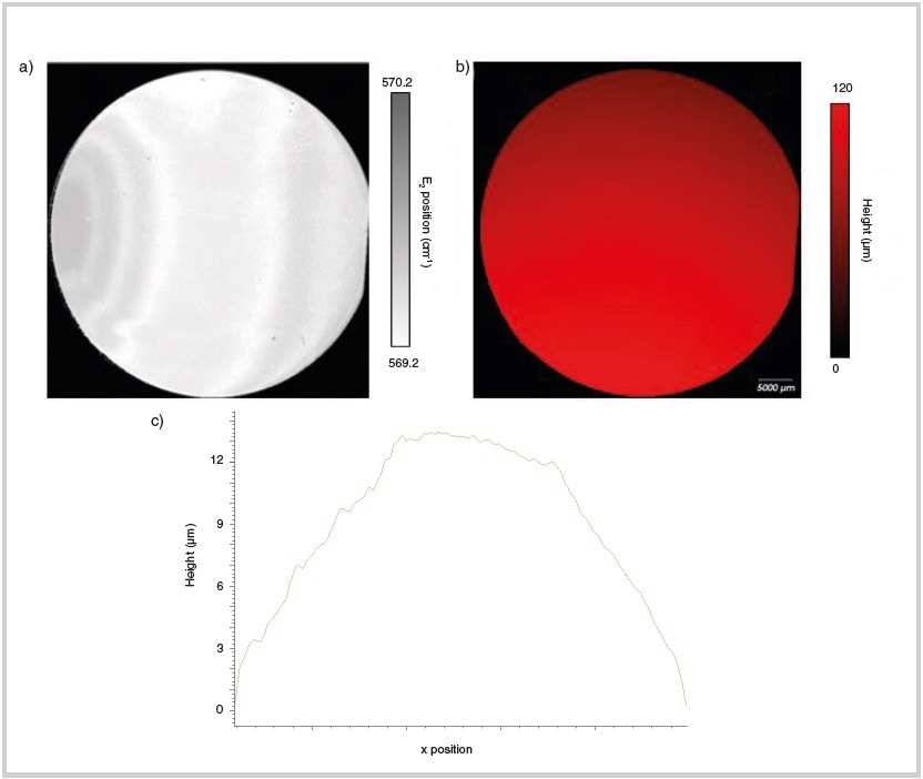
Figure 3. (a) Peak position of the E2 mode illustrating stress across the wafer, (b) topography image collected during Raman measurement, and (c) wafer bow (wafer tilt subtracted).
3D Microstructure and Stress Characterization of Novel GaN Structures
Threading dislocations in GaN-based semiconductors can behave as scattering centers for light as well as charge carriers. This behavior can hamper the semiconductors performance when in optoelectronic devices such as LEDs.
In-depth knowledge and characterization of the spatial distribution of threading dislocations gives researchers the ability to perform optimized layer growth using more innovative techniques. In this case, the microstructure and stress are characterized in a sample, grown using the epitaxial lateral overgrowth (ELOG) method, with the help of growth apertures that include a regular array of nano-dashes for controlling the coalescence process.
Raman measurements were performed with the help of a Renishaw inVia Qontor® Raman confocal microscope that includes a 150-mW, 532-nm laser excitation source. A typical spectrum obtained from the sample is shown in figure 4. After growth, 3D Raman data were obtained from the sample by focusing the laser at various depths. For the purposes of comparison, scanning electron microscope (SEM) images were obtained at the time of the growth process by disrupting the growth and moving the sample to an SEM. Figure 5 illustrates these images.
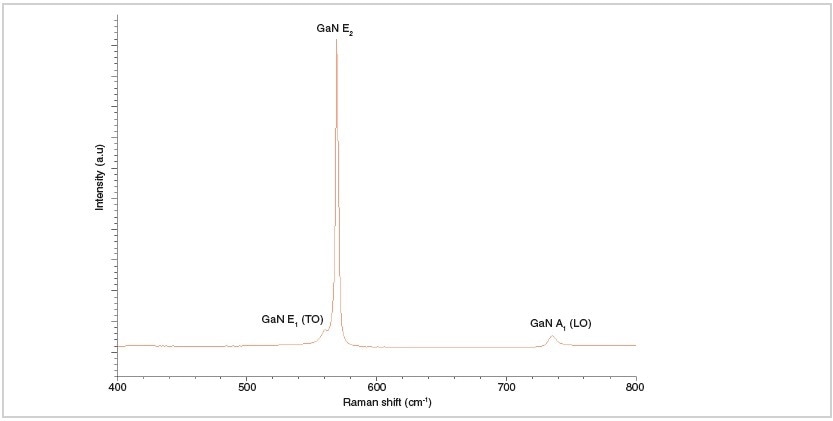
Figure 4. A typical spectrum from the novel nanostructure with GaN Raman modes labeled. The E1(TO) mode is present due to off-axis growth of the material.
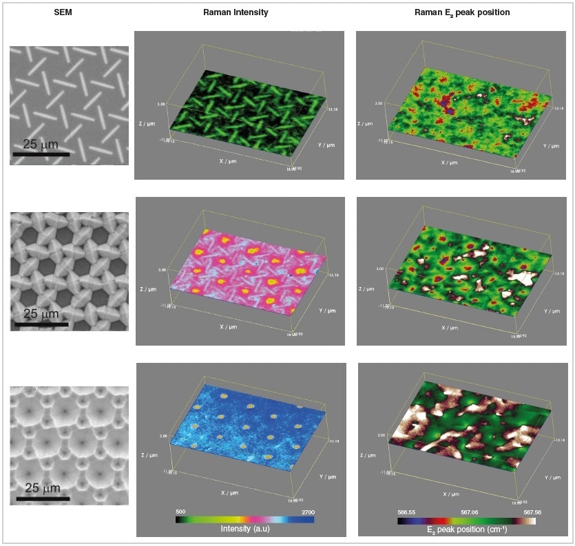
Figure 5. SEM and Raman images collected from the sample, z = 0 μm is the surface. Raman intensity images illustrate the microstructure of the sample and correlate well with the SEM images. The peak position of the E2 band moves toward the stress-free value at the surface. The Raman measurement area was 38.1 μm × 26.1 μm × 14 μm, with a step size of 0.3 μm × 0.3 μm × 2 μm.
The microstructure of the sample is clearly illustrated by the Raman intensity images, which also display regions of increased dislocation density and demonstrate excellent agreement with the SEM images. This shows that after growth, Raman can be used as an alternative for more complicated, interrupted growth and SEM analysis.
The distribution of stress in the sample can be investigated by examining the peak position of the E2 Raman band (figure 4), with a change of 2.7 cm−1 corresponding to 1 GPa. There is a distinct correlation between the stress distribution and the microstructure (intensity image) at a depth of −5 µm.
As shown in figure 6, approaching the suface, the peak position variation in the layer turns out to be more consistent and upshifts toward the anticipated stress-free value (567.5 cm−1). This shows that the innovative structure leads to a decrease in stress magnitude by concentrating the stress in the layer as designed.
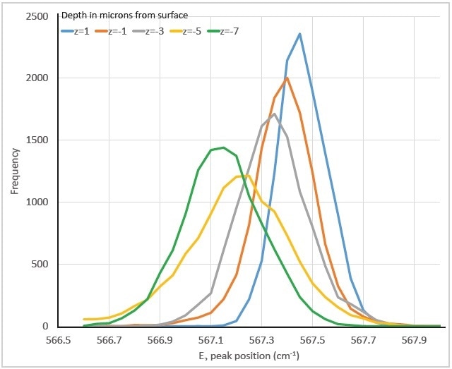
Figure 6. Histogram illustrating the variation in E2 peak position for different depths in the structure. The typical peak position upshifts toward the stress-free value 567.5 cm−1, and the distribution sharpens when moving from bulk to the surface of the sample.
Raman Thermography
A crucial parameter for evaluating the service life of the device is its peak operating device temperature. Conventional techniques (such as infrared (IR) and electrical measurements) offer poor spatial resolution and generally give average temperatures across the device, usually largely underestimating the peak temperature.
A pioneering study by Martin Kuball and colleagues has shown that Raman spectroscopy is an outstanding tool for the measurement of peak operational temperature in active devices in DC [1] as well as in pulsed mode [2].
Raman thermography operates on the principle that there is a change in the phonon energies of a material when there are changes in temperature. The change in Raman band positions for an on and pinched off high electron mobility transistor (HEMT) device is shown in figure 7. This change can be directly correlated to the temperature. When a Raman map is conducted over a device, its temperature distribution can be determined with sub-micron resolution.
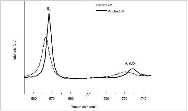
Figure 7. Comparison of Raman spectra for an on (hot) and pinched off device (cold).
The temperature distribution between the source drain for HEMTs grown on sapphire and SiC substrates is shown in figure 8. This figure illustrated that when the devices are operated at a peak temperature of 180 °C, devices on SiC can be operated at a power density more than three times. This is the result of the better thermal conductivity of SiC when compared to sapphire. Additionally, the device fabricated on sapphire exhibits a considerably flatter temperature distribution since the GaN has a higher thermal conductivity when compared to sapphire, leading to the preference of horizontal spreading of the heat than vertical extraction.
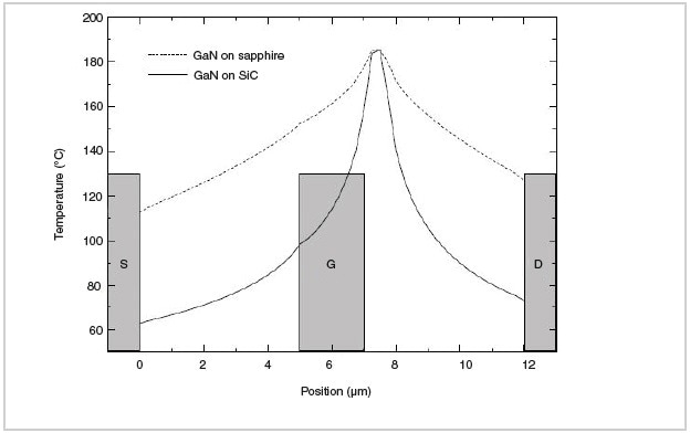
Figure 8. Temperature distribution of HEMTs fabricated on sapphire and SiC substrates. Devices were operated at different power densities to produce a peak temperature of 180 °C.
Conclusion
The examples above show the way in which the inVia Raman microscope can be adopted to analyze the following characteristics of compound semiconductors:
- PL
- Crystal structure
- Chemical composition
- Defects
- Stress/strain
- Device temperate
Users can contact their local Renishaw office for more information on the Renishaw inVia Raman microscope and its potential for being applied to compound semiconductors.
 Download the White Paper for More Information
Acknowledgements
The authors would like to thank Dr Emmanuel Le Boulbar, Professor Duncan Allsopp, and Professor Philip Shields from the University of Bath for offering the ELOG sample.
References
[1] Kuball, M., Hayes, J. M., Uren, M. J., Martin, I., Birbeck, J. C. H., Balmer, R. S., & Hughes, B. T. (2002). Measurement of temperature in active high-power AlGaN/GaN HFETs using Raman spectroscopy. IEEE Electron Device Letters, 23(1), 7-9.
[2] Kuball, M., Riedel, G. J., Pomeroy, J. W., Sarua, A., Uren, M. J., Martin, T., ... & Wallis, D. J. (2007). Time-resolved temperature measurement of AlGaN/GaN electronic devices using micro-Raman spectroscopy. IEEE electron device letters, 28(2), 86-89.

This information has been sourced, reviewed and adapted from materials provided by Renishaw plc.
For more information on this source, please visit Renishaw plc.